Introduction
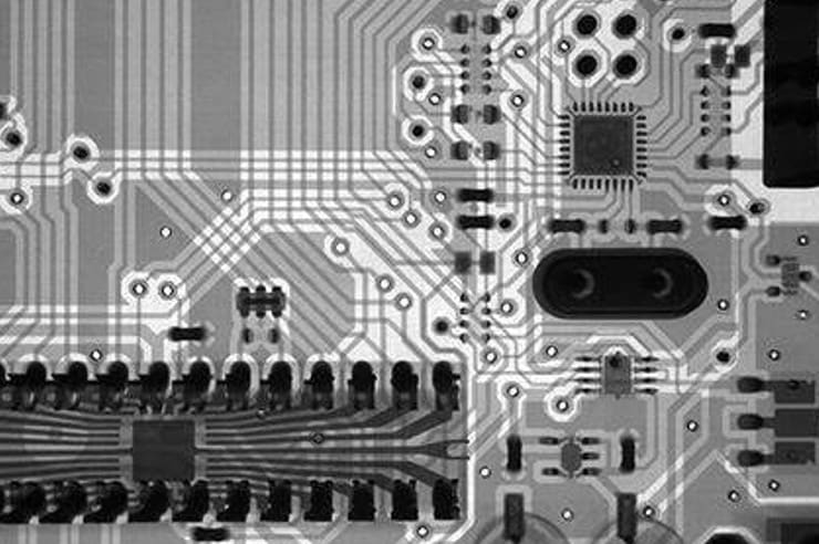
Printed circuit board (PCB) assembly processes have grown more complex with the rise of fine-pitch components and bottom-terminated devices like BGAs and QFNs. Traditional optical inspections often fall short in detecting hidden defects within solder joints or multilayer structures. Using X-Ray for PCB troubleshooting provides a non-destructive way to visualize these internal issues, enabling engineers to diagnose PCB failures with X-Ray imaging effectively. This approach reveals problems such as voids, bridges, and misalignments that could lead to field failures or unreliable performance. In high-volume production or prototype verification, mastering X-Ray analysis techniques becomes essential for maintaining quality and reducing rework costs. Engineers benefit from practical guidance on interpreting X-Ray images to make informed decisions quickly.
Why X-Ray Inspection Matters in PCB Assembly
X-Ray inspection stands out in PCB assembly because it penetrates opaque materials to expose defects invisible to the naked eye or automated optical systems. Components like ball grid arrays (BGAs) have solder joints hidden beneath the package, making surface checks inadequate for full verification. Diagnosing PCB failures with X-Ray helps identify issues early, preventing costly escapes to functional testing or customer sites. This method aligns with industry demands for higher reliability in electronics used in automotive, medical, and aerospace applications. Without it, assemblies risk intermittent failures from poor interconnections that degrade over time due to thermal cycling or vibration. Ultimately, integrating X-Ray into the workflow boosts yield rates and supports compliance with quality benchmarks.
The technique proves particularly valuable during reflow soldering stages where defects form due to process variations. Engineers can correlate X-Ray findings with process parameters like peak temperature or ramp rates to refine profiles. This targeted troubleshooting minimizes trial-and-error iterations in production lines.
Principles of X-Ray Imaging for PCBs
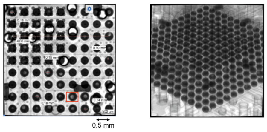
X-Ray systems generate a beam of low-energy radiation that passes through the PCB assembly, creating shadow images based on material density differences. Dense materials like copper and solder absorb more X-rays, appearing brighter, while air voids or low-density areas show as darker regions. Real-time 2D imaging offers quick overviews, but tilting the board or using oblique angles provides better separation of overlapping features. Advanced 3D computed tomography (CT) reconstructs layered slices for precise measurements, though it requires longer scan times suitable for failure analysis rather than inline inspection.
In practice, voltage settings around 50-130 kV balance penetration and resolution for typical board thicknesses. Tilt modes, often up to 60 degrees, help distinguish true bridges from shadows cast by adjacent balls. Understanding these principles ensures accurate using X-Ray for PCB troubleshooting without misreading artifacts.
Common PCB Assembly Failures Diagnosed with X-Ray
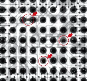
Solder voids rank among the most frequent defects, appearing as dark circular or irregular spots within joints due to outgassing during reflow. These reduce mechanical strength and thermal conductivity, potentially causing opens under stress. Bridging shows as unintended connections between adjacent joints, often from excess solder paste or poor stencil release. Head-in-pillow defects manifest as solder balls not fully wetting the pad, visible as offset or non-concentric shadows.
Missing or insufficient solder balls in BGAs create uniform dark areas under the package, signaling stencil printing or feeder issues. Barrel cracks in plated through-holes appear as linear dark lines along the via wall, stemming from plating voids or excessive drill smear. Component misalignment shifts joint shadows away from pad centers, complicating signal integrity.
Via fill problems in through-hole components reveal incomplete barrel coverage, critical for high-current paths. These failures underscore why diagnosing PCB failures with X-Ray remains indispensable for thorough assembly verification.
X-Ray Analysis Techniques for Troubleshooting
Engineers employ several X-Ray analysis techniques to pinpoint root causes systematically. Start with a full-board scan in orthogonal view to map high-risk areas like BGAs and QFNs. Then, apply tilt imaging to resolve overlapping features; a 45-degree angle often clarifies if a shadow indicates a true void or projection artifact. Oblique views from multiple angles enhance contrast for subtle issues like micro-cracks.
Quantitative measurements, such as void percentage, rely on grayscale thresholding to segment defects from solid solder. Slice reconstruction in 3D mode allows layer-by-layer inspection of multilayer boards, revealing interlayer shorts. Combining these with magnification zooms in on specific joints for detailed assessment.
According to IPC-7095 guidelines for BGA assemblies, specific criteria define acceptable joint fillet shapes and void limits observable via X-Ray. These techniques streamline using X-Ray for PCB troubleshooting in production environments.
Interpreting X-Ray Images: A Step-by-Step Guide
Begin interpreting X-Ray images by calibrating the system for consistent grayscale and adjusting voltage for optimal contrast. Scan the board systematically, starting from component outlines to verify placement before diving into joints. Look for uniform brightness in solder masses; deviations signal anomalies. Voids appear darker than surrounding material, with size and location noted against acceptance criteria.
Distinguish bridges by their continuous bright paths between joints, versus shadows from tilted balls which disappear at different angles. Head-in-pillow shows a ball diameter mismatch with the pad shadow. For vias, check barrel continuity; dark rings indicate plating discontinuities.
IPC-A-610 establishes visual criteria adaptable to X-Ray, such as maximum void diameter relative to ball size. Practice with known good and bad samples builds proficiency in spotting nuances.
Common X-Ray inspection errors include over-reliance on 2D views leading to false bridges, inadequate tilt causing overlap misreads, or ignoring board warpage that distorts projections. Always cross-verify with electrical testing to confirm findings.
Best Practices and Troubleshooting Tips
Adopt a multi-step workflow: pre-inspect with AOI for obvious issues, then X-Ray high-density areas. Train operators on image artifacts and standard criteria to minimize interpretation variability. Maintain equipment calibration per manufacturer specs to ensure repeatable results.
Integrate process feedback loops; for instance, excessive voids prompt stencil cleaning or paste viscosity checks. J-STD-001 outlines soldering requirements that correlate with X-Ray observables, guiding process adjustments.
Document findings with screenshots and measurements for yield analysis. Combine X-Ray with cross-sectioning for destructive confirmation on outliers. These practices enhance diagnosing PCB failures with X-Ray reliability.
In high-mix lines, prioritize inline automated X-Ray for speed, reserving manual systems for detailed troubleshooting.
Real-World Troubleshooting Examples
Consider a BGA package showing intermittent connectivity. X-Ray reveals 30% voids exceeding limits, traced to rapid ramp-up causing flux entrapment. Adjusting reflow profile resolved it.
Another case involves QFN bridges; oblique imaging confirmed solder extrusion from pad overflow, fixed by refining stencil apertures.
Via cracks in a multilayer board appeared post-shock test; 3D slices pinpointed drill-induced damage, prompting supplier process review.
These examples highlight practical application of interpreting X-Ray images for root cause isolation.
Conclusion
Mastering X-Ray for PCB troubleshooting empowers engineers to catch hidden defects early, ensuring robust assemblies. Key techniques like tilt imaging and void quantification, aligned with standards, drive precise diagnostics. Avoid common pitfalls through training and verification. Implementing these methods reduces rework, boosts yields, and upholds quality in demanding applications.
FAQs
Q1: What are the most common defects found when using X-Ray for PCB troubleshooting?
A1: Voids, solder bridges, head-in-pillow defects, and insufficient solder balls top the list, especially in BGAs and QFNs. These arise from reflow issues or printing errors. X-Ray clearly visualizes them by density contrasts, allowing quick identification and process tweaks for better yields. Always measure void sizes against criteria to classify severity.
Q2: How do you diagnose PCB failures with X-Ray in a production setting?
A2: Start with full-board scans, then focus on suspect areas using tilt for overlap resolution. Quantify defects like void percentages via software tools. Correlate findings with process data, such as thermal profiles. This non-destructive method fits inline workflows, minimizing downtime while catching issues optical inspection misses.
Q3: What techniques help in interpreting X-Ray images accurately?
A3: Use multi-angle views to eliminate shadows, grayscale adjustments for contrast, and 3D slicing for depth. Reference joint shapes against standards for acceptance. Practice distinguishes artifacts from true defects, ensuring reliable reads. Combine with electrical tests for validation.
Q4: What are common X-Ray inspection errors and how to avoid them?
A4: Misreading shadows as bridges or ignoring warpage distortions lead to false calls. Mitigate by standardizing tilt angles, calibrating regularly, and training on artifacts. Cross-checking with known samples builds confidence in X-Ray analysis techniques.
References
IPC-A-610H — Acceptability of Electronic Assemblies. IPC, 2020
IPC-7095D — Design and Assembly Process Implementation for BGAs. IPC, 2014
J-STD-001H — Requirements for Soldered Electrical and Electronic Assemblies. IPC, 2020


