What is Wave Soldering and Why is Process Control Important?
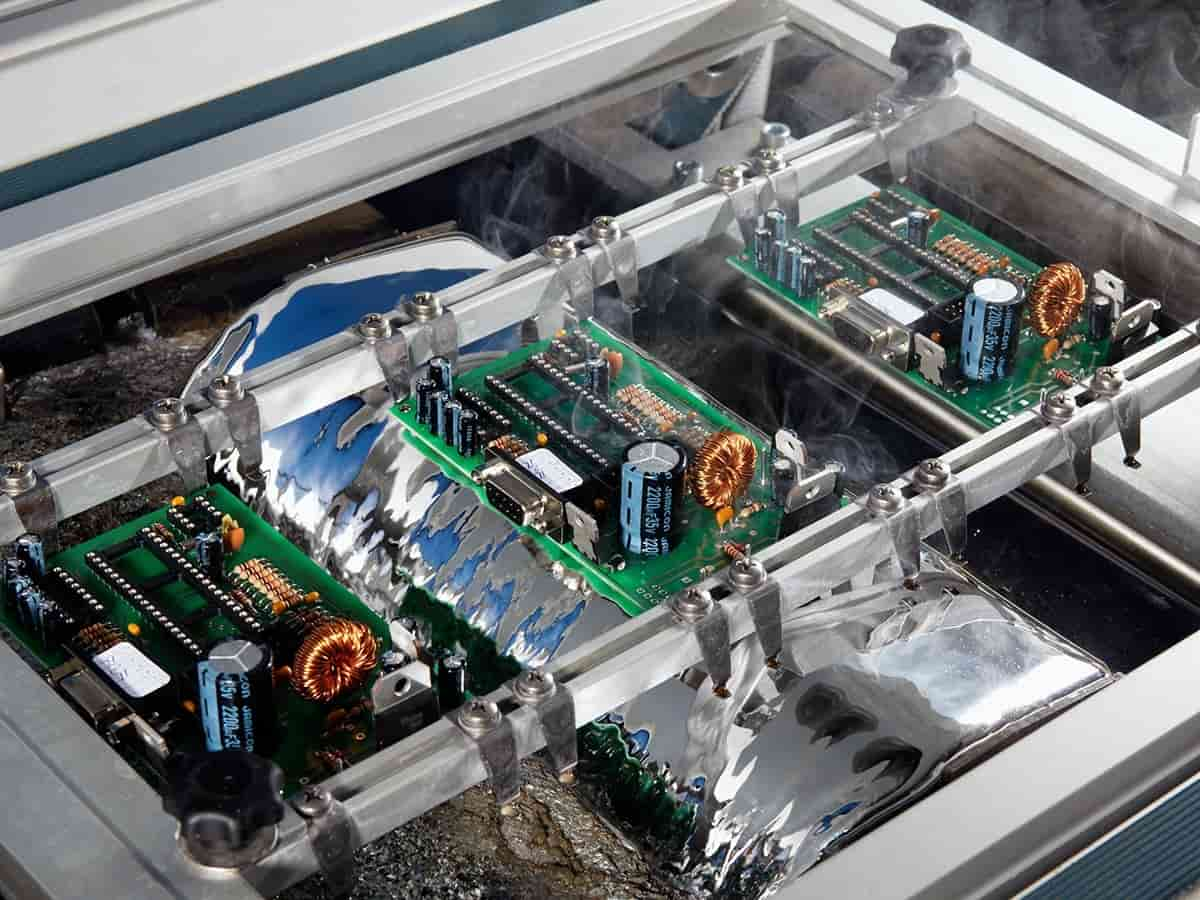
Wave soldering stands as a cornerstone method in electronics manufacturing, specifically tailored for efficiently attaching through-hole components to printed circuit boards (PCBs). This automated process involves passing a PCB over a carefully formed wave of molten solder, creating robust electrical and mechanical connections. Its speed and efficiency make it ideal for high-volume production lines. However, the complexity of the process also means that various issues can arise, impacting the quality of solder joints and the overall reliability of the finished board.
For engineers, a deep understanding of wave soldering and effective troubleshooting skills are essential. Defects can lead to costly rework, production delays, and compromised product performance. By mastering process control—meticulously monitoring and adjusting key parameters—engineers can significantly minimize defects and ensure consistent, high-quality output, thereby safeguarding product integrity and operational efficiency.
Common Wave Soldering Problems and Their Solutions
Wave soldering defects can originate from a variety of sources, ranging from incorrect machine settings to issues with board design or insufficient maintenance. This section details the most frequently encountered problems and offers practical, actionable solutions to address them.
Insufficient Hole Fill
This defect occurs when solder fails to fully penetrate a through-hole, resulting in a weak or incomplete connection that can lead to electrical failures.
● Causes: Inadequate preheat temperature (preventing proper solder flow), low solder wave height (not reaching the top of the PCB), or contaminated component leads (blocking solder adhesion).
● Solutions: Adjust preheat to 100-120°C; increase wave height to 2-3 mm above the board; ensure component leads are clean and flux is properly applied.
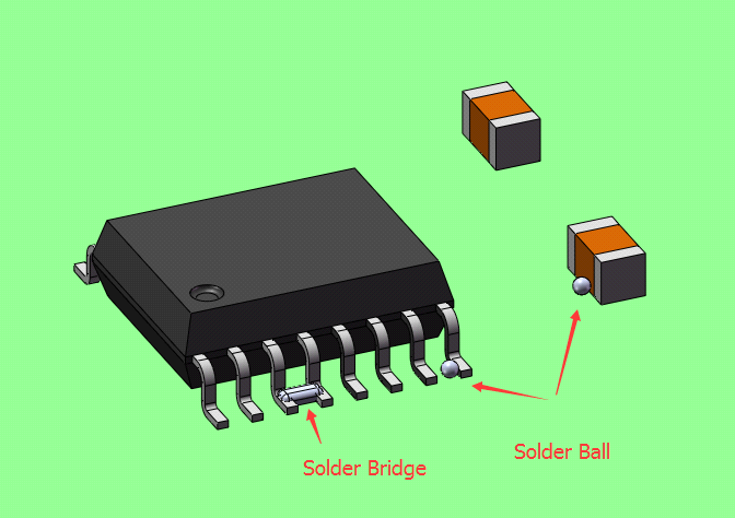
Solder Bridging
Solder bridging is the formation of unintended solder connections between adjacent pads or component leads, leading to short circuits.
● Causes: Excessive solder wave height or pressure (causing overflow), insufficient spacing between pads in the PCB design (less than 2.54 mm recommended), or uneven flux application (poor solder flow control).
● Solutions: Reduce solder wave height and pressure; review and adjust PCB layout for adequate spacing; optimize flux application for even coverage, targeting 500-1000 μg/in².
Cold Solder Joints
Cold solder joints appear dull, grainy, and often lumpy, indicating a poor metallurgical bond. These joints are mechanically weak and prone to failure.
● Causes: Low solder pot temperature (preventing proper melting and bonding, ideal 250-260°C for lead-free), insufficient dwell time in the solder wave (reducing heat transfer), or contaminated solder/flux.
● Solutions: Monitor and adjust solder pot temperature; slightly decrease conveyor speed to ensure 2-4 seconds dwell time; regularly test and replace contaminated solder or flux.
Solder Balling
This defect manifests as small, unwanted spheres of solder scattered across the PCB surface, which can cause shorts or aesthetic concerns.
● Causes: Excessive moisture on the board (causing solder splatter), high solder wave turbulence (generating droplets), or inadequate flux application (failing to control solder spread).
● Solutions: Pre-bake PCBs at 100°C for 1-2 hours to remove moisture; adjust wave pump speed for a smooth, laminar flow; ensure uniform flux application.
Suggested Reading: PCB Soldering Processes and Common Defects Explained
Lifted or Misaligned Components
Components that detach or shift during the soldering process lead to misalignment or completely failed connections.
● Causes: Excessive conveyor speed (dislodging components), poor component placement or insufficient adhesive before soldering, or thermal shock from rapid temperature changes.
● Solutions: Reduce conveyor speed (optimal 1-1.5 meters per minute); use appropriate adhesives or fixtures; optimize the preheat stage for a gradual temperature increase over 60-90 seconds to minimize thermal shock.
Essential Process Parameters for Consistent Wave Soldering Quality
Effective process control is the bedrock of defect-free wave soldering. By diligently monitoring and adjusting key parameters, engineers can preemptively tackle many common issues, ensuring consistent and high-quality assembly results.
● Solder Pot Temperature: Maintain the solder pot temperature within the recommended range for the solder alloy being used (e.g., 250-260°C for lead-free, 240-250°C for leaded). Verify daily with a calibrated digital thermometer.
● Preheat Temperature Profile: Ensure the PCB reaches an optimal preheat temperature (typically 100-120°C) before contacting the solder wave. This prevents thermal shock and facilitates even solder wetting.
● Solder Wave Height: Set the wave height precisely to 2-3 mm above the PCB surface to guarantee adequate contact without excessive overflow. Regular visual inspection of wave uniformity is critical.
● Conveyor Speed: Adjust the conveyor speed, usually between 1-1.5 meters per minute, to achieve the correct dwell time over the solder wave. This balances heat transfer and production throughput.
● Flux Application Uniformity: Ensure flux is applied evenly across the board, aiming for a density of 500-1000 μg/in². Use a flux residue test kit for verification if necessary.
By keeping these parameters within their specified ranges, the large PCB manufacturer can significantly reduce defect rates and elevate overall soldering quality.
Maintaining Your Wave Soldering Equipment for Peak Performance
Regular maintenance of wave soldering equipment is crucial for preventing downtime, ensuring consistent performance, and avoiding the array of defects caused by machine-related issues. Proactive maintenance is key to long-term success.
● Solder Pot Cleaning: Daily removal of dross (oxidized solder) from the pot is essential to prevent contamination. Weekly testing of solder composition should aim to keep impurities below 0.1%.
● Wave Nozzle Inspection: Inspect the wave nozzle weekly for any blockages or wear that could disrupt wave uniformity. Clean with non-abrasive tools as needed.
● Lubrication of Moving Parts: Monthly lubrication of conveyor belts and other mechanical components reduces wear and ensures smooth, consistent board movement.
● Fluxing System Care: Clean and refill the flux applicator at the beginning of each shift. Regularly inspect spray nozzles for clogs and replace them if they become worn or blocked.
● Heating Element Monitoring: Test the preheat and solder pot heaters bi-weekly to confirm they maintain accurate temperatures within ±5°C of their set points.
Establishing and adhering to a detailed maintenance schedule, with comprehensive activity logs, helps track equipment condition and identify potential issues before they escalate into production problems.
Conclusion: Mastering Wave Soldering for Quality Results
Wave soldering remains a key technique in high volume PCB assembly, offering both efficiency and precision when properly managed. However, challenges such as insufficient hole fill, solder bridging, and cold joints can compromise quality if not addressed. By applying the troubleshooting strategies discussed in this guide, you can effectively overcome these issues and enhance your overall soldering performance.
Consistent focus on wave soldering process control, equipment maintenance, and machine calibration is crucial for ensuring long-term reliability and minimizing defects. By implementing the preventive measures and best practices shared here, you’ll be able to achieve stable, high-quality solder joints across every production run. Continue monitoring parameters, maintaining your systems, and refining your workflow to keep your manufacturing at its best—with AIVON supporting your PCB assembly and soldering solutions.


