Introduction
In the realm of modern electronics, multi-layer PCB design has become a cornerstone for achieving high performance in complex circuits. At the heart of this design approach are power planes and ground planes, which play a critical role in maintaining signal integrity and ensuring noise reduction. These planes are not just layers of copper; they are essential for providing stable voltage distribution, minimizing electromagnetic interference, and supporting high-speed signals. For electrical engineers, understanding how to implement these planes effectively can mean the difference between a reliable product and one plagued by performance issues. This article explores the fundamental concepts of power and ground planes in multi-layer PCBs, their impact on PCB layout, and best practices to optimize circuit performance. Join us as we delve into the technical intricacies and practical applications of these vital design elements.
What Are Power and Ground Planes and Why Do They Matter
Power planes and ground planes are continuous layers of conductive material, typically copper, integrated into multi-layer PCB design. A power plane is dedicated to distributing a specific voltage level across the board, ensuring that components receive a stable and consistent supply. Conversely, a ground plane serves as a common reference point for all signals and provides a return path for currents, crucial for maintaining signal integrity. These planes are strategically placed within the stackup of a multi-layer PCB to reduce noise and electromagnetic interference.
Their importance cannot be overstated. Without proper implementation, circuits may suffer from voltage drops, crosstalk, or unwanted noise, all of which degrade performance. For high-speed designs, power and ground planes are indispensable for controlling impedance and minimizing loop areas, directly impacting noise reduction. They also aid in thermal management by dissipating heat across the board. For electrical engineers, mastering the use of these planes ensures robust and reliable PCB layouts, especially in applications like telecommunications, automotive systems, and industrial controls.
Technical Principles of Power and Ground Planes
Role in Signal Integrity
Signal integrity refers to the quality of an electrical signal as it travels through a PCB. Power and ground planes are fundamental to preserving this quality. By providing a low-impedance path for current return, ground planes reduce the loop area between signal traces and their return paths. A smaller loop area minimizes inductance, which in turn reduces noise and crosstalk in high-speed signals. Power planes, on the other hand, maintain a stable voltage supply, preventing fluctuations that could distort signals.
In multi-layer PCB design, placing a ground plane adjacent to signal layers creates a controlled impedance environment. This setup ensures that signals maintain their intended characteristics, avoiding reflections and timing issues. Standards like IPC-2221B, which covers generic design principles for printed boards, emphasize the importance of continuous planes to achieve optimal signal performance.
Impact on Noise Reduction
Noise reduction is another critical function of power and ground planes. Electrical noise, often caused by switching transients or electromagnetic interference, can disrupt circuit operation. A well-designed ground plane acts as a shield, absorbing and dissipating stray electromagnetic fields. It also provides a reference for decoupling capacitors, which filter out high-frequency noise from the power supply.
Power planes work in tandem with ground planes to form a low-impedance power distribution network. This configuration minimizes voltage ripples and ensures that components receive clean power. Splitting planes or introducing gaps can create high-impedance paths, leading to noise issues. Adhering to guidelines in standards like IPC-6012E, which addresses performance specifications for rigid boards, helps engineers avoid such pitfalls during PCB layout.
Related Reading: Power Plane Decoupling: A Comprehensive Guide to PCB Stability
Electromagnetic Compatibility Considerations
Electromagnetic compatibility is a key concern in modern electronics, and power and ground planes play a pivotal role. A continuous ground plane reduces radiated emissions by confining electric fields between signal layers and the plane itself. This containment prevents interference with nearby circuits or external devices. Power planes, when paired with proper decoupling, further minimize emissions by stabilizing the voltage supply.
In multi-layer PCB design, engineers must ensure that planes are unbroken wherever possible. Vias and cutouts can disrupt current flow, creating slots that act as antennas for electromagnetic radiation. Following best practices outlined in IPC-A-600K for board acceptability ensures that plane integrity is maintained, supporting both signal integrity and noise reduction.
Best Practices for Implementing Power and Ground Planes
Optimal Stackup Configuration
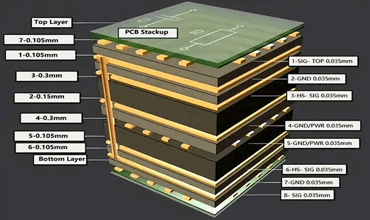
The arrangement of layers in a multi-layer PCB, known as the stackup, significantly affects performance. A common practice is to sandwich signal layers between ground planes or between a power plane and a ground plane. This configuration provides a return path for signals and shields them from interference. For a four-layer board, a typical stackup might include a top signal layer, a ground plane, a power plane, and a bottom signal layer.
Ensuring symmetry in the stackup prevents warping during manufacturing, as noted in IPC-6012E. Engineers should also prioritize placing high-speed signal traces adjacent to ground planes to control impedance. For complex designs with multiple voltage levels, split power planes can be used, but care must be taken to avoid overlapping splits with critical signal paths.
Decoupling and Capacitor Placement
Decoupling capacitors are essential for noise reduction in power distribution networks. These components should be placed as close as possible to the power pins of integrated circuits, with their ground connections tied directly to the ground plane through vias. This minimizes inductance and ensures effective filtering of high-frequency noise.
Capacitor values should be chosen based on the frequency range of expected noise. Multiple capacitors with different values can be used to cover a broad spectrum. Standards like JEDEC J-STD-020E provide guidelines on component handling that indirectly influence capacitor placement and reliability in PCB layout.
Minimizing Plane Interruptions
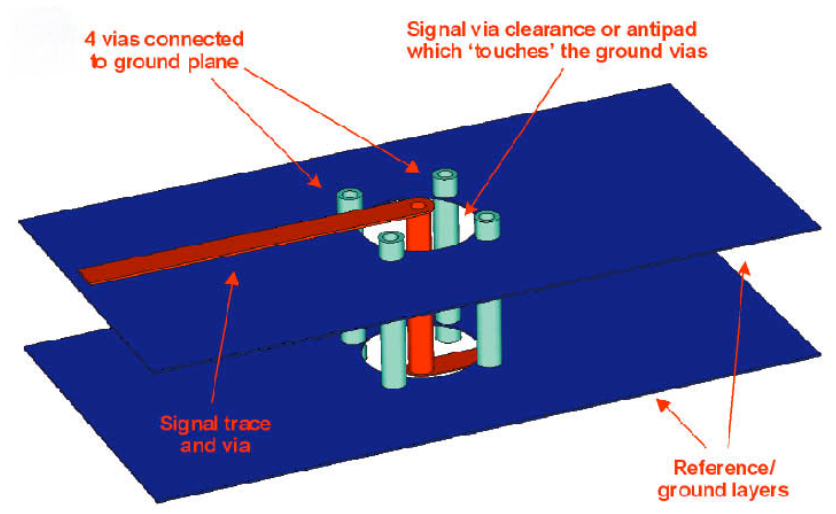
Interruptions in power and ground planes, such as slots or large cutouts, can disrupt current flow and degrade performance. When vias or connectors must pass through planes, they should be surrounded by stitching vias to maintain continuity. This technique, often referred to as via stitching, reduces impedance and prevents the formation of radiating slots.
For split planes used to accommodate multiple voltage levels, transitions between different power domains should be carefully managed. Signals crossing these splits require reference plane continuity, often achieved by placing stitching capacitors across the split. Following IPC-2221B recommendations helps ensure that such design choices do not compromise signal integrity.
Thermal and Current Distribution
Power planes also serve as heat sinks, distributing thermal energy across the board. Engineers must ensure that the copper thickness of these planes is adequate to handle the expected current load without excessive heating. Ground planes similarly aid in thermal management by providing a large conductive area for heat dissipation.
Current density should be analyzed during the design phase to avoid hotspots. Standards like IPC-2152 provide guidance on current-carrying capacity for copper traces and planes, ensuring safe and efficient power distribution in multi-layer PCB design.
Troubleshooting Common Issues with Power and Ground Planes
In practice, engineers often encounter challenges related to power and ground planes that affect signal integrity and noise reduction. One common issue is inadequate decoupling, leading to voltage fluctuations. This can be resolved by reviewing capacitor placement and values, ensuring they are optimized for the circuit’s frequency requirements.
Another frequent problem is plane resonance, where the power and ground planes form a parallel plate capacitor that resonates at specific frequencies. This can amplify noise in the system. Adding damping resistors or using multiple decoupling capacitors with staggered values can mitigate this effect. Additionally, ensuring that planes are continuous and free from large gaps prevents resonance from becoming a significant issue.
Crosstalk between signal traces due to improper plane referencing is also a concern. If a signal trace crosses a split in a reference plane, it may lose its return path, leading to noise. Rerouting traces to avoid splits or adding stitching vias can resolve this. Referencing IPC-A-600K during inspection ensures that manufacturing defects do not exacerbate such problems.
Related Reading: High Frequency PCB Routing Techniques: Minimizing Signal Loss and Interference
Conclusion
Power and ground planes are indispensable elements of multi-layer PCB design, directly influencing signal integrity and noise reduction. By providing stable voltage distribution, low-impedance return paths, and shielding against interference, these planes ensure the reliable operation of complex circuits. Electrical engineers must carefully consider stackup configurations, decoupling strategies, and plane continuity to optimize performance. Adhering to industry standards and best practices allows for the creation of robust PCB layouts that meet the demands of high-speed and high-power applications. With a thorough understanding of these principles, designers can tackle the challenges of modern electronics, achieving both efficiency and reliability in their projects.
FAQs
Q1: How do ground planes improve signal integrity in multi-layer PCB design?
A1: Ground planes in multi-layer PCB design provide a low-impedance return path for signals, reducing loop inductance and minimizing crosstalk. They maintain a consistent reference voltage, ensuring signals are not distorted by noise or reflections. Placing signal layers adjacent to ground planes also controls impedance, vital for high-speed circuits. This setup preserves signal quality across the board.
Q2: What is the role of power planes in noise reduction for PCB layouts?
A2: Power planes distribute stable voltage across the PCB, preventing fluctuations that introduce noise. Paired with decoupling capacitors, they filter high-frequency disturbances, ensuring clean power delivery to components. A continuous power plane reduces impedance, minimizing voltage ripples. This is crucial for noise reduction in sensitive electronic designs.
Q3: Why is stackup important for power and ground planes in PCB design?
A3: Stackup determines the placement of power and ground planes relative to signal layers, impacting signal integrity and electromagnetic compatibility. A well-designed stackup, with ground planes near signal layers, controls impedance and shields against interference. It also ensures balanced thermal and mechanical properties, preventing issues during manufacturing and operation.
Q4: How can engineers avoid issues with split planes in multi-layer PCB design?
A4: Engineers can avoid split plane issues by ensuring signals do not cross splits without a reference path. Stitching capacitors or vias near splits maintain continuity for return currents. Careful planning of power domains and trace routing prevents impedance mismatches. Following established design guidelines helps mitigate risks associated with split planes.
References
IPC-2221B — Generic Standard on Printed Board Design. IPC, 2012.
IPC-6012E — Qualification and Performance Specification for Rigid Printed Boards. IPC, 2020.
IPC-A-600K — Acceptability of Printed Boards. IPC, 2020.
IPC-2152 — Standard for Determining Current Carrying Capacity in Printed Board Design. IPC, 2009.
JEDEC J-STD-020E — Moisture/Reflow Sensitivity Classification for Nonhermetic Surface Mount Devices. JEDEC, 2014.