Introduction
In the fast-paced world of PCBs production lines, maintaining high assembly quality is essential for reliable electronic products. In-Circuit Testing, commonly known as ICT, serves as a cornerstone in this process by providing detailed diagnostics on assembled boards. Electric engineers rely on insights from an In-Circuit testing machine to verify component integrity and interconnection reliability right after surface-mount technology placement and soldering. This testing method uncovers potential issues that could lead to field failures, ensuring compliance with production standards. By examining electrical parameters at the node level, ICT reveals the health of the In-Circuit PCB before it advances to functional validation. Ultimately, it bridges the gap between manufacturing and performance assurance in high-volume environments.
What Is In-Circuit Testing and Why Does It Matter?
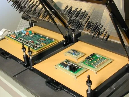
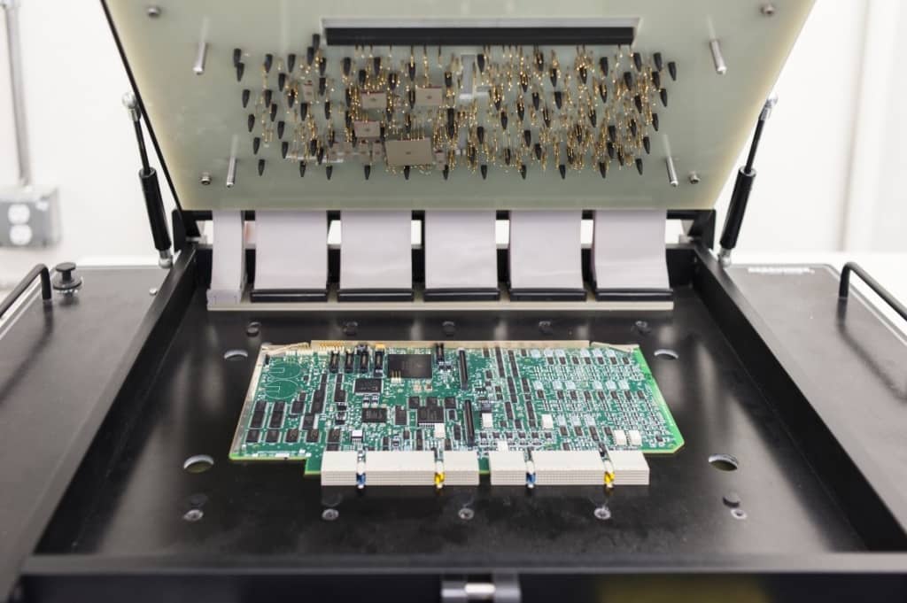
In-Circuit Testing involves probing specific points on an assembled printed circuit board to measure passive and active component values while isolating surrounding circuitry. Typically performed using a bed-of-nails fixture or flying probe system, it applies low-level stimuli to check for deviations from expected specifications. This approach targets manufacturing defects that automated optical inspection might miss, such as hidden solder joint problems. For electric engineers overseeing PCBs production lines, ICT matters because it achieves high fault coverage, often exceeding 90 percent for assembly-related issues, without powering the full board. It enables pinpointing of faults to individual components or nets, reducing debug time and scrap rates. In high-reliability applications, this testing aligns with factory quality gates, preventing downstream rework costs.
The relevance of ICT extends to its role in process control within the PCBs production line. Data from In-Circuit testing machines feeds into statistical process control charts, highlighting trends like reflow profile inconsistencies or feeder malfunctions. Engineers use these insights to refine pick-and-place accuracy or stencil alignment. Without ICT, latent defects could propagate, compromising product yield and customer satisfaction. Standards like IPC-A-610 provide criteria for acceptable assembly features that ICT verifies electrically. Thus, it transforms raw production data into actionable intelligence for continuous improvement.
Technical Principles of In-Circuit Testing
At its core, ICT operates by establishing electrical continuity between test probes and designated access points on the In-Circuit PCB. The system Guardian software models the netlist derived from the assembly design, comparing measured values against golden board baselines or tolerance bands. For passive components, it performs digital voltmeter tests for resistors, capacitor checks via AC stimulation, and diode forward voltage drops. Inductors and transformers receive specialized vector measurements to assess turns ratios. Active devices like transistors undergo parametric sweeps to confirm gain and threshold levels. This node-by-node isolation prevents interference from adjacent circuits, ensuring precise diagnostics.
Fault detection in ICT revolves around common assembly anomalies. Open circuits appear as infinite resistance between connected nodes, often due to lifted pads or missing vias. Shorts manifest as near-zero resistance across insulators, signaling solder bridges or debris. Component presence verifies through continuity to pins, while value mismatches flag wrong parts or drift from thermal stress. Polarity errors in diodes or capacitors trigger asymmetric responses under stimulus. Solder joint integrity shows via contact resistance exceeding thresholds, indicating cold joints or voids. These measurements, executed in seconds per board, provide a comprehensive electrical map of the assembly.
Advanced ICT systems incorporate boundary scan for digital ICs, complementing analog tests per J-STD-001 soldering requirements. Vectorless techniques like nodal analysis detect opens without fixtures, ideal for double-sided boards. Test coverage depends on access points, typically requiring 80 to 95 percent of nets probed. Engineers optimize probe density to balance fixture complexity and throughput in PCBs production lines. Environmental controls, such as fixture temperature stabilization, minimize measurement drift from thermal expansion. Overall, these principles ensure ICT delivers factory-grade verification aligned with engineering specifications.
Integrating ICT into the PCBs Production Line
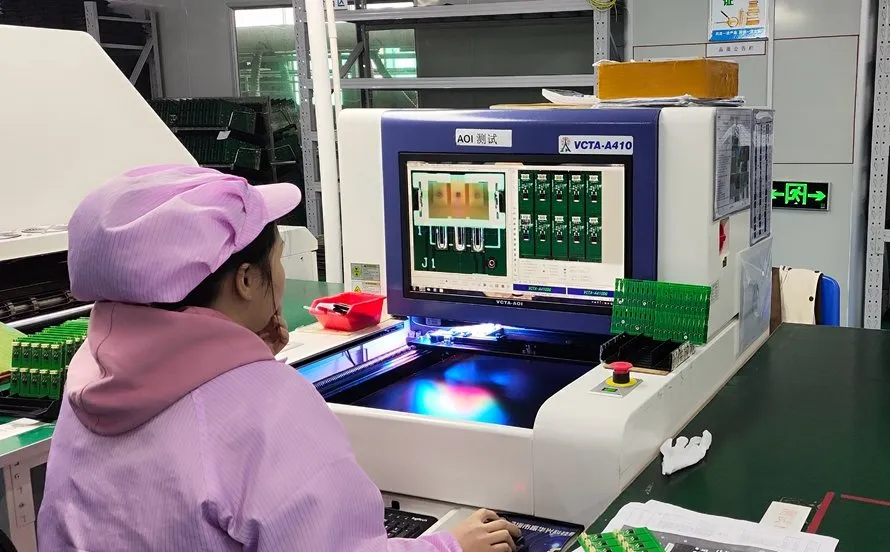
Positioning an In-Circuit testing machine post-reflow and pre-conformal coating optimizes the PCBs production line flow. Boards transfer via conveyor to the tester, where automated alignment ensures repeatable probe contact. High-volume lines employ parallel fixtures for throughput exceeding 100 units per hour. Data logging captures yield metrics, correlating fails to upstream processes like paste printing. Electric engineers analyze this telemetry to adjust oven profiles or component tolerances proactively. Seamless integration reduces handling damage and supports just-in-time manufacturing.
Fixture design proves critical for reliable ICT outcomes. Mechanical alignment pins match board fiducials, while spring-loaded probes deliver 50 to 100 grams of force per point. Vacuum hold-down secures warped boards, preventing intermittent contacts. Software simulation predicts probe interference, adhering to IPC-2221 guidelines for testability. Custom kelvin connections enhance low-resistance measurements for power nets. Regular maintenance, including probe cleaning and wear inspection, sustains accuracy across shifts. These elements make ICT a robust link in the production chain.
Best Practices for Maximizing ICT Insights
Electric engineers should prioritize design for testability from the schematic stage to maximize In-Circuit PCB diagnostics. Incorporate 0.5 mm test pads on every net, spaced at least 1.27 mm apart to avoid crosstalk. Use guard traces around sensitive analog sections to isolate measurements. Limit component density near edges for fixture clearance. Simulate test programs during layout to verify coverage gaps. These practices, rooted in factory experience, boost first-pass yields.
In operation, calibrate In-Circuit testing machines daily against reference standards to account for probe degradation. Set tolerances at three sigma for parametric tests, allowing for process variation. Implement auto-learn for golden boards to baseline new revisions. Train operators on fault codes for rapid triage, directing fails to visual or X-ray stations. Integrate with manufacturing execution systems for real-time dashboards. Periodic audits against IPC-A-610 criteria validate test limits.
Troubleshooting common ICT pitfalls enhances line efficiency. Fixture misalignment causes mass opens; recalibrate Z-axis travel. High capacitance fails signal dirty probes; ultrasonic cleaning resolves this. Component tolerance drifts from binning errors require supplier audits. Software glitches manifest as inconsistent vectors; update netlists from gerber revisions. By addressing these systematically, engineers extract maximum value from ICT data.
Troubleshooting Insights from ICT Data
Factory-driven analysis of ICT fails reveals patterns in PCBs production line weaknesses. Clusters of resistor high fails point to dry joints from inadequate flux, prompting paste recipe tweaks. Capacitor shorts often trace to tombstoning, adjustable via ramp-soak profiles. IC parametric drifts indicate ESD exposure, necessitating better handling protocols. Mapping fails spatially uncovers stencil wear hotspots. Engineers leverage this granularity for root cause countermeasures.
Case in point, a production run showed elevated via opens on inner layers. ICT nodal tests isolated the issue to via-in-pad drilling misalignment. Correlating with cross-section analysis confirmed barrel cracks. Adjusting drill peck cycles per J-STD-001 resolved recurrence. Such diagnostics underscore ICT's role beyond pass-fail, as a process sentinel.
Conclusion
In-Circuit Testing stands as an indispensable tool for electric engineers, revealing the true state of assembled PCBs in production lines. From detecting basic connectivity issues to validating complex parametric behaviors, ICT ensures manufacturing defects do not compromise reliability. Adhering to standards like IPC-A-610 and IPC-2221 fortifies its effectiveness. By integrating best practices and thorough troubleshooting, factories achieve superior yields and robust products. Ultimately, the insights from an In-Circuit testing machine empower informed decisions, bridging design intent with production reality.
FAQs
Q1: What faults does ICT primarily detect on an In-Circuit PCB?
A1: ICT on an In-Circuit testing machine identifies opens, shorts, missing or wrong components, incorrect values, and poor solder joints. It measures resistance, capacitance, and diode characteristics to isolate these assembly defects. In PCBs production lines, this high fault coverage prevents faulty boards from advancing. Engineers use the data for immediate rework, aligning with quality standards.
Q2: How does an In-Circuit testing machine integrate into PCBs production lines?
A2: An In-Circuit testing machine positions post-reflow for optimal defect catch. Automated conveyors feed boards into bed-of-nails fixtures for rapid nodal testing. Yield data feeds process controls, enabling real-time adjustments. Electric engineers monitor throughput and fault trends to refine upstream steps like soldering.
Q3: Why is test point placement critical for In-Circuit PCB testing?
A3: Proper test points ensure probe access without interference, maximizing coverage in In-Circuit testing. Per IPC-2221 guidelines, pads on every net facilitate accurate measurements. Poor placement leads to blind spots, reducing diagnostic power. Factory best practices include simulating probe paths during design.
Q4: Can ICT replace functional testing in production?
A4: No, ICT focuses on component-level verification, while functional testing checks system behavior. In-Circuit testing machines excel at manufacturing defects but miss intermittent issues. Combining both in PCBs production lines provides comprehensive assurance. Engineers prioritize ICT for high-volume efficiency.
References
IPC-A-610H — Acceptability of Electronic Assemblies. IPC, 2020
IPC-2221B — Generic Standard on Printed Board Design. IPC, 2012
J-STD-001G — Requirements for Soldered Electrical and Electronic Assemblies. IPC/JEDEC, 2011


