Introduction
In-Circuit Testing, commonly known as ICT, serves as a cornerstone in PCB assembly quality control processes within manufacturing facilities. This method systematically verifies the functionality of individual components and interconnections on assembled printed circuit boards before they proceed to final integration. Factory engineers rely on ICT to detect defects early, minimizing rework costs and ensuring compliance with rigorous production standards. The ICT principle revolves around precise electrical measurements using specialized fixtures, making it indispensable for high-volume electronics production. By isolating and stimulating specific nodes, ICT provides detailed diagnostics that support efficient troubleshooting in a factory environment.
What Is In-Circuit Testing and Why It Matters
In-Circuit Testing involves placing an assembled PCB onto a custom fixture that establishes electrical contact with numerous test points simultaneously. This approach allows testers to evaluate components like resistors, capacitors, diodes, and transistors in their operational context without removing them from the board. Unlike visual inspections or automated optical checks, ICT delivers quantitative data on electrical performance, confirming that solder joints and nets meet expected parameters. In factory settings, where throughput is critical, ICT achieves high test coverage, often addressing the majority of assembly-related faults.
The relevance of ICT stems from its ability to bridge bare board testing and full functional validation. Manufacturing teams implement it to align with quality benchmarks, reducing field failures in electronic products. For electric engineers overseeing production lines, understanding the ICT principle ensures optimized test strategies that balance speed and accuracy. Defects such as open circuits, shorts, or incorrect component values, if undetected, can cascade into system-level issues downstream.
Core Technical Principles of In-Circuit Testing
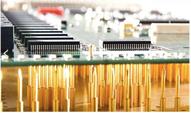
The fundamental ICT principle centers on the bed of nails fixture, an array of spring-loaded probes precisely aligned to contact designated test points on the PCB surface. These points include component leads, vias, and dedicated test pads designed into the layout for optimal access. When the fixture actuates, it presses the board down, creating reliable low-resistance connections across hundreds or thousands of nodes. The test system then references a predefined netlist, which maps expected interconnections, to perform guided measurements.
Testing proceeds in phases, starting with power-off tests to safeguard sensitive components. During power-off evaluation, the system injects low-level DC or AC signals into isolated nodes and measures parameters like resistance for continuity checks or capacitance for passive verification. Guarding techniques play a key role here, where adjacent nodes are virtually grounded to prevent interference from parallel paths, ensuring accurate readings of the device under test. This method effectively identifies solder defects, wrong polarities, or missing parts without applying operational voltages.
Power off test specifically targets passive elements and basic connectivity. Engineers configure it to sweep nets for opens and shorts by comparing measured resistances against thresholds derived from the bill of materials. For instance, a resistor's value is confirmed by forcing a small current and sensing voltage drop, while capacitors undergo charging/discharging cycles. These factory-driven procedures align with standards like IPC-A-610, which define acceptability criteria for electronic assemblies.
Once power-off passes, the system transitions to powered tests, applying controlled voltages to analog and digital circuits. Transistor base-emitter junctions receive forward bias to verify switching characteristics, while IC pin states are probed for logic levels. Parametric limits, programmed based on component datasheets, flag deviations, providing pinpoint fault isolation. The bed of nails enables parallel access, drastically reducing test times compared to sequential probing methods.
Advanced ICT systems incorporate vector-based testing for digital devices, simulating clock signals to exercise flip-flops and gates. Analog sections undergo stimulus-response analysis, such as frequency sweeps for filters. Throughout, software algorithms correlate results against the golden board profile—a reference from a known-good unit—to automate pass/fail decisions. This principled approach ensures comprehensive coverage while adhering to J-STD-001 requirements for soldered electrical connections.

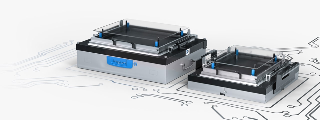
Fixture Design and Test Program Development
Effective ICT implementation begins with fixture engineering tailored to the PCB's geometry and component density. Factory teams position probes at vias or pads with at least 0.5 mm spacing to avoid crosstalk, incorporating mechanical supports to prevent board flexure during contact. Vacuum hold-downs or pneumatic presses maintain consistent pressure, ensuring probe penetration through any oxidation layers. Alignment fiducials on the PCB guide precise placement, critical for high-density boards.
Test program generation follows a structured workflow, starting with CAD data import to auto-populate the netlist. Engineers refine probe assignments, prioritizing high-failure nets from historical data. Parametric models for components account for tolerances, setting guard relays to isolate clusters effectively. Simulation software verifies test sequences pre-build, reducing fixture iterations in production.
Best practices include allocating 5-10% of board area to test points, placed near suspect-prone areas like BGA corners. Compliance with IPC-A-610 ensures that test-induced stresses do not compromise assembly integrity. Regular fixture maintenance, such as probe cleaning and spring calibration, sustains measurement repeatability across shifts.
Troubleshooting Common ICT Failures
In factory troubleshooting, power off test failures often point to assembly issues like insufficient solder volume or tombstoning. Engineers review waveforms for erratic resistances, correlating with X-ray if vias are implicated. Shorts between adjacent nets trigger fixture checks for probe misalignment or board warpage. Component value drifts suggest thermal stress during reflow, prompting process audits.
Powered test anomalies require isolating analog versus digital domains. For example, a failing op-amp output might stem from open feedback paths, verified by re-probing subsets. Data logging enables trend analysis, linking failures to specific lots per ISO 9001 quality management principles. Collaborative reviews between test and process engineers accelerate root cause resolution.
Conclusion
The ICT principle, underpinned by the bed of nails fixture and phased testing like power off evaluations, delivers factory-grade assurance for PCB assemblies. Electric engineers benefit from its precision in verifying components and nets against standards such as IPC-A-610 and J-STD-001. By integrating accessible test points and robust programming, manufacturers achieve high yields and reliability. As production scales, ICT remains a vital tool, evolving with denser boards while upholding quality fundamentals.
FAQs
Q1: What is the ICT principle in PCB testing?
A1: The ICT principle involves using a bed of nails fixture to make multiple electrical contacts with the PCB, applying stimuli to measure component values and net continuity. Power off tests isolate passives without voltage risks, followed by functional checks. This factory method ensures assembly integrity per IPC-A-610 criteria, detecting most defects efficiently.
Q2: How does the bed of nails work in In-Circuit Testing?
A2: The bed of nails consists of spring-loaded pins aligned to PCB test points, enabling simultaneous access for measurements. When actuated, it guards nodes to prevent interference during resistance or capacitance checks. Ideal for high-volume production, it supports rapid power off test execution, aligning with J-STD-001 soldering standards.
Q3: What is a power off test in ICT?
A3: Power off test in ICT evaluates opens, shorts, and passive components like resistors and capacitors without board power-up. Low signals probe nets against the netlist, identifying solder issues early. This safe, preliminary step boosts fault coverage in factory lines, complementing visual inspections under IPC-A-610.
Q4: Why is ICT important for electric engineers in manufacturing?
A4: ICT provides quantifiable data on assembly quality, reducing escapes to final test. Its bed of nails and power off test phases enable quick isolation, supporting ISO 9001 compliance. Engineers optimize designs for testability, ensuring reliable production scaling.
References
IPC-A-610H — Acceptability of Electronic Assemblies. IPC, 2019
J-STD-001GS — Requirements for Soldered Electrical and Electronic Assemblies. IPC, 2020
ISO 9001:2015 — Quality Management Systems. ISO, 2015


