Introduction
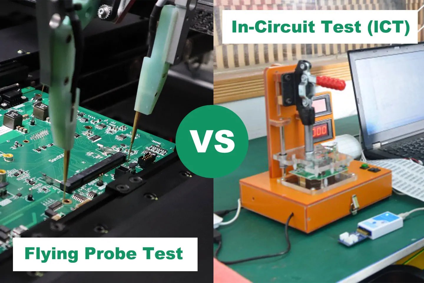
In-circuit testing stands as a cornerstone in ensuring the electrical integrity and functionality of assembled printed circuit boards. Electric engineers often face the decision between bed-of-nails testers and flying probe testers when implementing in-circuit testing strategies. Bed-of-nails testers provide rapid, parallel testing through a fixed fixture, while flying probe testers offer flexibility with movable probes. This choice impacts production throughput, cost efficiency, and adaptability to design changes. Understanding the strengths of each method helps engineers select the optimal approach for their specific production needs. Factory-driven insights reveal that aligning tester selection with volume requirements and design stability yields the highest reliability outcomes.
The Fundamentals of In-Circuit Testing
In-circuit testing verifies the performance of individual components and interconnections on an assembled PCB without removing them from the board. It detects faults such as opens, shorts, wrong component values, and soldering defects by applying stimuli and measuring responses at designated test points. This method complements visual inspections and functional tests, providing comprehensive coverage early in the production process. Electric engineers value in-circuit testing for its ability to isolate issues at the component level, reducing debug time downstream. Standards like IPC-9252 outline requirements for electrical testing, ensuring consistency across manufacturing environments. Proper implementation minimizes escapes to field use, upholding product quality.
How Bed-of-Nails Testers Work
Bed-of-nails testers employ a custom fixture embedded with hundreds of spring-loaded probes arranged to contact specific test points on the PCB underside. When the board is pressed onto the fixture, all probes make simultaneous electrical contact, enabling parallel measurement of resistances, capacitances, and other parameters. The tester applies power and signals through these probes to check component values in-circuit while guarding against interference from adjacent circuits. Test cycles complete in seconds, making this method ideal for high-speed production lines. Fixture design requires precise engineering to align with PCB layout, including provisions for mechanical support and vacuum hold-down. Engineers must account for probe density limits, typically supporting up to 10,000 points, to cover complex boards effectively.
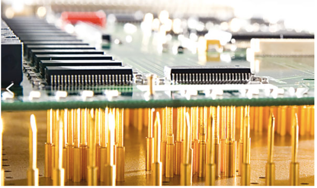
Advantages and Limitations of Bed-of-Nails Testers
The primary advantage of bed-of-nails testers lies in their unparalleled test speed and repeatability for high-volume runs. Once the fixture is built, per-board testing costs drop significantly, supporting thousands of units per day without reconfiguration. This parallelism excels in detecting subtle faults across dense boards, aligning with factory goals for throughput. However, the high non-recurring engineering cost for fixture fabrication, often requiring weeks of lead time, poses challenges for prototypes or evolving designs. Mechanical wear on probes and fixtures demands regular maintenance to prevent false calls. Design changes necessitate fixture redesigns, amplifying costs in agile development cycles.
Principles Behind Flying Probe Testers
Flying probe testers use two or four independently controlled robotic probes that move precisely across the PCB surface to access test points sequentially. Advanced vision systems guide probe placement with micron accuracy, compensating for board warpage or component misalignment. Each probe pair handles measurements like continuity, insulation resistance, and component verification, often accessing both sides without flipping the board. Test programs generate automatically from CAD data, reducing setup time compared to fixture-based systems. This fixtureless approach suits low-volume production where flexibility trumps speed. Engineers appreciate the ability to program boundary scans or powered tests on the fly, enhancing diagnostic depth.
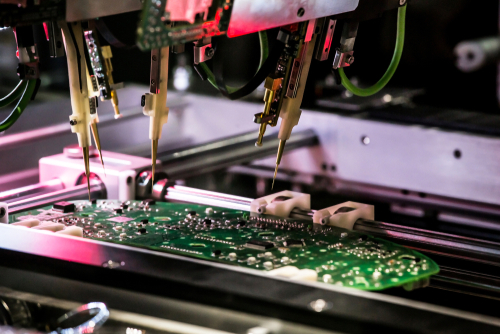
Strengths and Drawbacks of Flying Probe Testers
Flying probe testers shine in their zero fixture cost and rapid adaptability to design revisions, making them perfect for new product introductions. They handle double-sided boards and irregular shapes effortlessly, with probe counts limited only by machine kinematics. High accuracy reduces false positives, and software-driven test development accelerates time-to-market. On the downside, sequential testing extends cycle times to minutes per board, limiting throughput to dozens per hour. Complex boards with thousands of nets may require optimized probe paths to avoid excessive wear. Factory insights indicate that flying probe testers excel when combined with automated optical inspection for hybrid strategies.
Key Differences Between Bed-of-Nails and Flying Probe Testers
-
Test Speed — Bed-of-Nails: Seconds per board (parallel); Flying Probe: Minutes per board (sequential)
-
Upfront Cost — Bed-of-Nails: High (custom fixture); Flying Probe: Low (no fixture)
-
Volume Suitability — Bed-of-Nails: High-volume production; Flying Probe: Low to medium volume, prototypes
-
Flexibility — Bed-of-Nails: Low (design changes costly); Flying Probe: High (quick reprogramming)
-
Probe Access — Bed-of-Nails: Fixed, underside primarily; Flying Probe: Movable, both sides
-
Maintenance — Bed-of-Nails: Fixture/probe wear; Flying Probe: Probe tips, less frequent
This comparison highlights how bed-of-nails testers prioritize efficiency in stable, mass production, while flying probe testers emphasize versatility. Electric engineers use such metrics to model return on investment based on run sizes. Fixture-based systems offer better parallelism for dense nets, but flying probes provide superior access to guarded or high-density areas. Production data consistently shows bed-of-nails yielding higher uptime in dedicated lines. Selecting based on these factors ensures alignment with manufacturing constraints.
When to Choose Bed-of-Nails Testers
Opt for bed-of-nails testers in high-volume scenarios where production exceeds hundreds of boards daily and designs remain stable post-prototyping. Mature products with fixed test point layouts benefit from the fixture's reliability, minimizing operator intervention. Factories producing consumer electronics or automotive modules leverage this for cost-per-unit savings after amortizing fixture expenses. Ensure PCB designs incorporate sufficient test points per IPC-6012 specifications to maximize coverage. This method suits environments demanding Class 3 assembly reliability, where J-STD-001 compliance verifies soldering integrity through electrical checks. Avoid it for pilot runs, as fixture iterations erode budgets quickly.
Scenarios Ideal for Flying Probe Testers
Flying probe testers prove essential for prototypes, low-volume custom boards, or frequent engineering changes common in R&D phases. They enable quick validation of new component libraries or layout tweaks without tooling delays. In factories handling diverse SKUs, the lack of dedicated fixtures streamlines changeovers between jobs. Engineers testing high-mix, low-volume medical devices or aerospace prototypes rely on their precision for comprehensive netlist verification. Pairing with functional test reduces overall validation time despite slower cycles. This approach scales well up to medium volumes, transitioning to bed-of-nails only when throughput bottlenecks emerge.
Design Considerations for Testability
Effective in-circuit testing begins with design for testability, allocating 20 to 50 test points per square inch depending on density. Place vias or dedicated pads at accessible locations, avoiding BGA shadows or tight component pitches. Guard traces isolate analog sections during digital tests, preventing crosstalk. Software simulation predicts fault coverage, guiding probe assignments. Compliance with IPC guidelines ensures probe force and spacing prevent board damage. Electric engineers iterate layouts using DFT rules to balance testability with routing constraints.
Best Practices in Factory Implementation
Integrate bed-of-nails or flying probe testers into a layered test strategy, following bare board E-test with in-circuit verification. Calibrate systems daily to maintain measurement accuracy within specified tolerances. Train operators on error codes for rapid fault isolation, reducing mean time to repair. Log test data for trend analysis, identifying process drifts early. Hybrid flows, using flying probe for NPI and bed-of-nails for volume, optimize costs across lifecycles. Adhering to standards like IPC-9252 during fixture design guarantees robust electrical interfaces.
Real-World Decision Insights
Consider a high-volume consumer router production: bed-of-nails testers achieve 99.5% uptime with 2-second cycles, justifying $20,000 fixture investment over 50,000 units. Conversely, for a custom industrial controller with quarterly revisions, flying probe testers cut setup to hours, avoiding repeated fixture costs. Engineers in automotive suppliers favor bed-of-nails for AEC-Q100 compliance testing, ensuring zero defects at speed. Prototyping teams in telecommunications use flying probe for 4-8 layer boards, validating RF sections inaccessible via fixtures. These scenarios underscore volume and stability as primary discriminators. Factory metrics guide transitions, often at 500-1000 units per design.
Conclusion
Choosing between bed-of-nails testers and flying probe testers hinges on production volume, design maturity, and cost tolerances in in-circuit testing workflows. Bed-of-nails excel in high-throughput environments with stable designs, delivering speed and repeatability. Flying probe testers offer unmatched flexibility for prototypes and low-volume runs, adapting seamlessly to changes. Electric engineers benefit from evaluating these factors alongside test coverage goals and factory constraints. Implementing best practices and standards ensures reliable outcomes, minimizing field failures. Ultimately, the right tester elevates PCB quality control to meet demanding industry expectations.
FAQs
Q1: What are the main advantages of bed-of-nails testers over flying probe testers in in-circuit testing?
A1: Bed-of-nails testers provide ultra-fast parallel testing, completing cycles in seconds for high-volume production. They offer high repeatability and low per-unit costs after fixture amortization. This suits stable designs in factories prioritizing throughput. However, they require custom tooling unsuitable for prototypes. Standards-aligned implementation maximizes fault detection efficiency.
Q2: When should electric engineers prefer flying probe testers for PCB in-circuit testing?
A2: Flying probe testers are ideal for low to medium volumes, prototypes, or designs with frequent changes due to no fixture costs and quick reprogramming. They access both board sides easily, handling complex geometries. Test times of minutes per board fit NPI phases perfectly. Factory insights recommend them for high-mix environments. Coverage remains comprehensive with proper netlist programming.
Q3: How do bed-of-nails testers and flying probe testers compare in terms of cost for in-circuit testing?
A3: Bed-of-nails testers incur high upfront fixture costs but low ongoing expenses for large runs. Flying probe testers eliminate tooling fees, favoring small batches economically. Engineers calculate breakeven around 500 units based on test time and labor. Volume drives the choice in production planning. Both deliver reliable in-circuit testing when matched correctly.
Q4: What role do industry standards play in selecting bed-of-nails or flying probe testers?
A4: Standards like IPC-9252 guide electrical test requirements, influencing fixture design for bed-of-nails or probe accuracy for flying probes. They ensure consistent fault detection across methods. Compliance supports Class 2 or 3 assemblies reliably. Engineers reference them for test point allocation and measurement tolerances. This alignment boosts manufacturing quality control.
References
IPC-9252B — Requirements for Electrical Testing of Unpopulated Printed Boards. IPC, 2016
IPC-6012E — Qualification and Performance Specification for Rigid Printed Boards. IPC, 2017
J-STD-001H — Requirements for Soldered Electrical and Electronic Assemblies. IPC, 2020


