Introduction
Surface mount technology (SMT) has revolutionized electronics manufacturing by enabling higher component densities and smaller form factors. However, the complexity of modern assemblies introduces challenges that traditional optical inspections cannot fully address. SMT x-ray inspection emerges as a critical quality control tool, revealing defects hidden beneath components and within solder joints. This non-destructive method ensures reliability in high-stakes applications like automotive and medical devices. By penetrating materials to visualize internal structures, x-ray inspection for surface mount processes bridges the gap between visible surfaces and concealed interconnections. Factory engineers rely on it to maintain compliance and minimize field failures.
What Is SMT X-Ray Inspection and Why It Matters
SMT x-ray inspection, also known as automated x-ray inspection (AXI), uses high-energy photons to generate images of PCB assemblies. These X-rays pass through the board, creating contrast based on material density, where solder appears bright due to high atomic number elements like tin and copper. Unlike automated optical inspection (AOI), which is limited to surface features, x-ray inspection penetrates opaque packages to inspect hidden solder joints in components such as ball grid arrays (BGAs) and quad flat no-leads (QFNs). This capability is essential for detecting issues that compromise electrical conductivity, thermal performance, and mechanical integrity.
The relevance of SMT x-ray inspection stems from the shift toward fine-pitch, bottom-terminated components in modern electronics. Defects invisible to the eye, like voids or bridging under a BGA, can lead to intermittent failures under thermal cycling or vibration. In high-volume production, integrating x-ray inspection reduces rework costs and enhances yield rates. Factories achieve better process control by correlating x-ray data with reflow profiles and stencil designs. Ultimately, it supports adherence to industry benchmarks for assembly quality, ensuring products meet end-user reliability demands.
Principles of X-Ray Inspection in SMT
X-ray inspection operates on the principle of differential absorption, governed by the Beer-Lambert law, where transmitted intensity decreases exponentially with material thickness and density. Photons in the 30 to 160 keV range penetrate FR-4 substrates and silicon dies with minimal attenuation but are strongly absorbed by lead-free solders like SAC305. This creates grayscale images: voids appear as dark spots, full solder joints as bright areas, and copper traces as intermediate gray. Systems adjust tube voltage based on board thickness, typically 60 to 90 kV for standard 1.6 mm PCBs, to optimize contrast without overpenetration.
Two primary types dominate SMT applications: 2D and 3D systems. 2D x-ray provides single-angle projections for rapid inline screening, achieving resolutions of 3 to 5 microns at speeds of 60 to 200 boards per hour. It excels in high-volume environments but struggles with overlapping features in multilayer assemblies. 3D computed tomography (CT) reconstructs volumetric data from multiple angles, offering sub-micron resolution and slice views for precise defect sizing. Factories select based on throughput needs, reserving 3D for failure analysis or complex boards.
Resolution depends on focal spot size, detector technology like amorphous silicon panels, and magnification up to 1000 times. Quantitative analysis measures void percentages, solder volume, and joint fillet heights directly from images. Operators interpret these alongside qualitative shapes, such as hourglass forms indicating head-in-pillow defects. This technical foundation enables factories to quantify process variations and implement data-driven improvements.
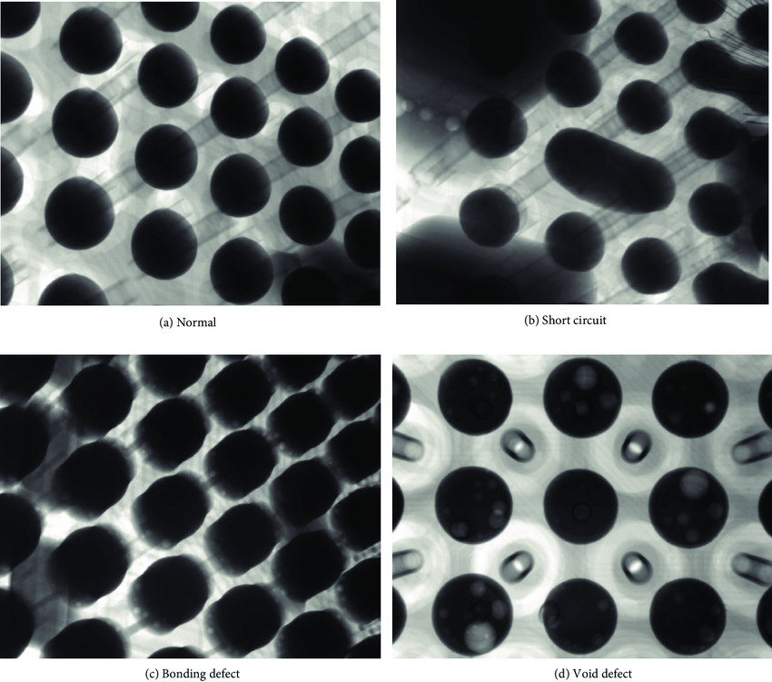
Key Defects Detected by SMT X-Ray Inspection
SMT defect detection via x-ray focuses on hidden solder joint issues that AOI misses. Voids, trapped gas pockets in reflowed solder, reduce thermal conductivity and create stress risers, often exceeding 25 percent of joint area in non-compliant joints. Bridging manifests as bright white connections between pads, risking shorts in dense arrays. Head-in-pillow defects show partial separation between solder balls and paste deposits, forming weak interfaces prone to fatigue. These anomalies arise from flux entrapment, warpage, or oxidation during reflow.
Component placement x-ray verifies alignment offsets, ensuring less than 50 percent electrode width deviation per class 2 criteria. Misplaced BGAs or QFNs lead to open joints or uneven wetting, visible as spherical balls or starved fillets. Insufficient solder volume appears as low grayscale density, while excess causes bloating or protrusions violating clearances. Internal cold joints exhibit grainy textures from poor wetting, increasing resistance. Factories prioritize these scans post-reflow to catch process drifts early.
Under-component bridging and thermal pad voiding in QFNs compromise grounding and heat dissipation, with voids over 20 to 30 percent signaling stencil or paste issues. X-ray also reveals via barrel cracks or delamination in multilayers, though less common in pure SMT. By isolating these, engineers trace root causes like reflow profiles or paste rheology. Regular monitoring prevents escalation to functional failures.
Solder Paste Inspection and Component Placement with X-Ray
Solder paste inspection (SPI) traditionally uses optical methods, but x-ray enhances volume and height measurements for hidden deposits. It quantifies paste height uniformity across pads, detecting insufficient release from stencils as low-density areas. Bridging in paste appears early, allowing pre-reflow corrections. This step integrates seamlessly before placement, correlating with joint quality post-reflow. Factories use x-ray SPI selectively for fine-pitch apertures under 0.3 mm to predict void risks.
Component placement x-ray confirms offsets and rotations invisible externally. For BGAs, it checks ball-to-pad registry, flagging shifts beyond tolerance. QFN and LGA scans verify peripheral lead wetting and central pad coverage. Multiple angles, like oblique and right-angle views, confirm fillet formation and absence of lifted leads. This verifies pick-and-place accuracy, reducing downstream defects.
In production, x-ray feedback loops optimize machine parameters, such as nozzle vacuum or vision alignment. Statistical process control tracks placement Cpks alongside x-ray metrics. Engineers adjust for warpage-induced shifts, ensuring consistent yields.
Best Practices for X-Ray Inspection in SMT Production
Implement a layered strategy: AOI for surfaces, x-ray for hidden joints. Conduct 100 percent x-ray on critical components like BGAs in high-reliability builds, sampling stable lines at 10 to 20 percent. Inline 2D systems maintain throughput, offline 3D for root cause analysis. Train operators per IPC-A-610 criteria, focusing on void quantification and marginal calls. Correlate x-ray data with ICT results to validate electrical integrity.
Position boards consistently, using fixtures for repeatability. Scan multiple views: center, corners, and sides for comprehensive coverage. Automate defect classification with software thresholds, achieving over 99 percent accuracy. Adjust processes based on trends, like widening stencil apertures for high-void rates. Per J-STD-001, verify hidden joints meet wetting and fill requirements.
Integrate x-ray into the factory floor post-pick-and-place, SPI, and reflow gates. Maintain equipment with daily calibration checks on resolution and dosage. Document images with heatmaps for supplier audits. This factory-driven approach aligns with IPC-7095 guidelines for BGA processes, minimizing escapes.
Troubleshooting Common SMT X-Ray Findings
High void rates often trace to reflow ramp rates or paste volatility. Slow soaks trap gases; engineers extend profiles or switch alloys. Head-in-pillow signals warpage mismatches; pre-bake boards or select low-alpha flux. Bridging under QFNs points to overprint; refine squeegee pressure.
Misalignment clusters indicate vision system drift; recalibrate feeders. Quantitative x-ray metrics guide SPC charts, flagging excursions. Cross-section samples validate x-ray calls for process tuning. Factories build libraries of defect signatures for rapid diagnosis.
Conclusion
SMT x-ray inspection stands as an indispensable tool for uncovering hidden defects in surface mount assemblies. From voids and bridging to placement errors, it delivers actionable insights beyond optical limits. Adhering to standards like IPC-A-610 ensures consistent quality across production runs. Factories gain process mastery, boosting yields and reliability. As component densities rise, x-ray integration will only grow in importance for electric engineers optimizing workflows.
FAQs
Q1: What defects does SMT x-ray inspection primarily detect?
A1: SMT x-ray inspection excels at identifying hidden issues like solder voids, bridging, head-in-pillow defects, and insufficient wetting in BGA and QFN joints. These compromise joint integrity, which AOI cannot see. Factories use it post-reflow for quantitative analysis, measuring void percentages against class criteria. This prevents thermal and mechanical failures in field use.
Q2: How does x-ray inspection for surface mount improve over AOI?
A2: X-ray penetrates components to visualize internal structures, unlike AOI's surface-only view. It detects subsurface bridging, voids, and misalignment in bottom-terminated parts. Production lines pair them for full coverage, with x-ray verifying AOI flags. This combination enhances defect detection rates in high-density SMT.
Q3: When should solder paste inspection use x-ray methods?
A3: Use x-ray for solder paste inspection on fine-pitch stencils to measure volume and bridging accurately. It complements optical SPI by revealing density variations pre-reflow. Factories apply it selectively for void-prone processes, adjusting print parameters accordingly. This proactive step minimizes post-reflow rework.
Q4: What role does component placement x-ray play in SMT defect detection?
A4: Component placement x-ray confirms alignment offsets and rotations for hidden leads, flagging shifts that cause opens. Multiple angles ensure pad registry in QFNs and BGAs. Integrated with SPC, it tunes pick-and-place accuracy. Engineers rely on it for zero-escape quality in complex assemblies.
References
IPC-A-610 — Acceptability of Electronic Assemblies. IPC
IPC J-STD-001 — Requirements for Soldered Electrical and Electronic Assemblies. IPC
IPC-7095 — Design and Assembly Process Implementation for BGAs. IPC


