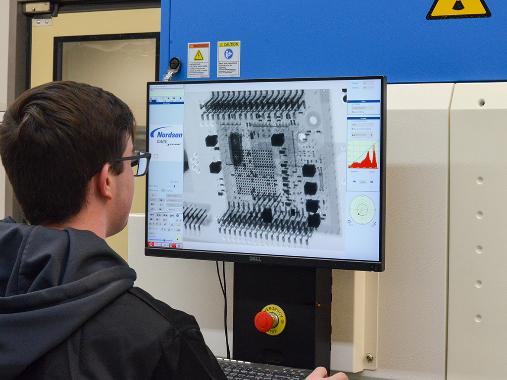
Introduction
In electronics manufacturing, ensuring the reliability of printed circuit boards (PCBs) demands precise detection of hidden defects that optical inspection methods often miss. X-ray inspection emerges as a critical technology, providing non-destructive visibility into internal structures like solder joints and vias. This approach addresses PCB manufacturing defects that compromise performance, such as voids or misalignments beneath components. For electric engineers focused on quality control, mastering X-ray applications means bridging the gap between production speed and defect-free assemblies. As manufacturing scales to support high-density interconnects, integrating X-ray systems becomes essential for maintaining standards compliance and operational efficiency. Ultimately, this technology transforms defect detection from a reactive process to a proactive strategy.
Why X-Ray Inspection Matters in PCB Manufacturing
Traditional visual and automated optical inspections excel at surface-level checks but fall short for subsurface issues prevalent in modern PCBs. X-ray machines penetrate materials like FR-4 laminates and solder masks to reveal anomalies invisible to the naked eye. This capability proves vital in high-volume production where defects like internal voids can lead to field failures, escalating costs and delays. Electric engineers appreciate how X-ray inspection aligns with factory-driven quality goals, enabling early intervention before assembly completion. By identifying issues at the bare board or populated stage, manufacturers reduce rework and scrap rates. In essence, X-ray adoption directly correlates with improved PCB yield, a key metric for competitive electronics fabrication.
Technical Principles of X-Ray Inspection for PCBs
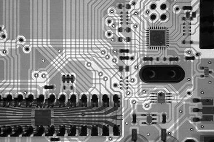
X-ray inspection relies on the differential absorption of X-rays by materials, where denser elements like copper and solder appear brighter on the image compared to lighter substrates. Transmission X-ray systems project a beam through the PCB onto a detector, generating 2D grayscale images that highlight density variations. For more complex boards, oblique-angle or laminography techniques provide pseudo-3D views by tilting the board or source, reducing overlap from multi-layer features. Advanced 3D computed tomography (CT) reconstructs volumetric data through multiple projections, offering slice-by-slice analysis ideal for dense BGAs. Engineers must consider factors like kV settings and exposure time to balance penetration depth with resolution, avoiding artifacts from board thickness. These principles ensure accurate representation of internal geometries without physical sectioning.
Resolution in X-ray systems typically reaches microns, sufficient for detecting via fills or joint fillet formations. Source focal spot size influences image sharpness, with microfocus tubes preferred for fine-pitch components. Detector types, such as flat-panel amorphous silicon arrays, convert X-rays to digital signals for real-time processing. Software algorithms enhance images through edge detection and automated defect classification, streamlining operator review. In practice, electric engineers calibrate systems based on board stack-up to optimize contrast for specific materials.
Common Defect Types Detected by X-Ray
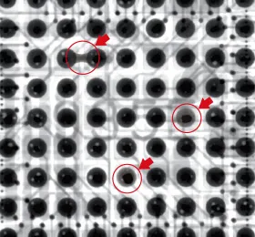
PCB manufacturing defects span a range from bare board fabrication to final assembly, with X-ray excelling at those hidden within layers. Voids in plated through-holes (PTHs) manifest as dark circular regions, indicating incomplete plating that risks open circuits under thermal stress. Solder joint defects in BGAs include head-in-pillow, where the solder ball fails to fully wet the pad, visible as offset grayscale intensities. Bridging between adjacent joints appears as unintended conductive paths, potentially shorting signals.
Misaligned components or insufficient solder volume show as asymmetric joint profiles, critical for reliability in vibration-prone applications. Cracks in copper traces or barrels from drilling stress reveal as linear density disruptions. Barrel pull-away at the knee of PTHs, a common plating issue, presents as gaps between copper and board edge. X-ray also flags foreign inclusions like solder balls or debris trapped under masks.
For electric engineers, understanding these defect types detected by X-ray informs root cause analysis, linking them to upstream processes like plating chemistry or reflow profiles.
X-Ray Inspection Standards and Guidelines
Adhering to established standards ensures X-ray results contribute meaningfully to quality assurance. IPC-A-610 provides criteria for solder joint acceptability, including void limits in BGAs that X-ray verifies non-destructively. This standard classifies defects by class, guiding thresholds for commercial versus high-reliability boards. Similarly, IPC-7095 outlines design and process controls for BGAs, emphasizing inspection techniques like X-ray for post-reflow validation.
Engineers apply these in factory settings by establishing acceptance criteria, such as maximum void percentage per joint. Calibration protocols maintain system accuracy, correlating X-ray findings with cross-sections for validation. Integrating X-ray data into statistical process control monitors trends in defect rates across lots.
Best Practices for Implementing X-Ray Inspection
To maximize X-ray machine applications, factories position systems post-fabrication, post-SMT, and pre-conformal coating for comprehensive coverage. Automating tilt sequences captures multi-angle data, essential for stacked die or cavity boards. Operators train on image interpretation, distinguishing true defects from artifacts like fiber weave shadows.
Programming regions of interest (ROIs) focuses scans on high-risk areas like BGAs or fine-pitch QFNs, optimizing throughput. Combining X-ray with AOI creates hybrid workflows, where optical flags trigger detailed X-ray review. Regular maintenance, including tube replacement and detector cleaning, sustains performance.
Electric engineers benefit from data logging for yield analytics, correlating defects to process parameters. Threshold setting evolves with experience, balancing false calls against escapes.
Improving PCB Yield with X-Ray Inspection
X-ray inspection directly boosts PCB yield by enabling process feedback loops that minimize escapes. Early detection of via defects post-drill and plate prevents costly assembly scrapping. In SMT lines, real-time X-ray halts production for bridging issues, preserving material.
Yield improvements stem from targeted corrections, like adjusting plating current for barrel voids. Factories report yield gains through reduced rework, as X-ray quantifies defect populations for DOE experiments. Long-term, it supports supplier qualification by auditing incoming boards.
For high-mix environments, flexible X-ray setups handle prototypes to volume runs. Engineers leverage metrics like defects per million opportunities (DPMO) to benchmark progress.
Troubleshooting Common X-Ray Challenges
Electric engineers often encounter image quality issues from board warpage, addressed by fixturing or dual-source systems. Overlapping features in multilayer boards require laminography to disentangle signals. Quantitative analysis, like void volume calculation, demands precise calibration against known standards.
Software glitches or noise from high-speed scans resolve via filtering algorithms. Integrating X-ray with metrology tools verifies measurements like via diameter. Persistent challenges yield to systematic DOE, refining parameters for specific board types.
Conclusion
X-ray inspection stands as an indispensable tool for mastering defect detection in PCB manufacturing, unveiling issues that threaten reliability. From voids and misalignments to solder anomalies, it covers critical defect types detected by X-ray across the production chain. Compliance with standards like IPC-A-610 and IPC-7095 ensures consistent application, while best practices drive yield enhancements. Electric engineers gain factory-level insights, optimizing processes for superior outcomes. Embracing this technology fortifies electronics manufacturing against hidden flaws, paving the way for robust, high-performance assemblies.
FAQs
Q1: What are the main PCB manufacturing defects that X-ray inspection can detect?
A1: X-ray excels at identifying subsurface issues like voids in vias and PTHs, BGA solder joint anomalies such as head-in-pillow, bridging, and insufficient fill. It reveals cracks, misalignments, and barrel pull-away invisible to optical methods. Factory implementation focuses scans on high-risk areas, correlating findings to process adjustments for better control.
Q2: How do X-ray machine applications improve PCB yield?
A2: By providing non-destructive internal views, X-ray enables early defect detection post-fabrication and assembly, reducing rework and scrap. Yield rises through data-driven tweaks to plating, reflow, and drilling. Engineers track metrics like DPMO, achieving sustained gains in high-volume lines.
Q3: What X-ray inspection standards should electric engineers follow?
A3: Key standards include IPC-A-610 for joint acceptability and IPC-7095 for BGA processes, defining void limits and classification. These guide criteria setting and validation against cross-sections. Factories align protocols to ensure compliance across production classes.
Q4: Which defect types detected by X-ray are most critical for high-reliability PCBs?
A4: Critical defects encompass via voids risking opens, solder cracks under thermal cycling, and foreign particles causing shorts. X-ray quantifies severity, prioritizing fixes per IPC guidelines. Proactive scanning prevents field failures in demanding applications.
References
IPC-A-610H — Acceptability of Electronic Assemblies. IPC, 2019
IPC-7095D — Design and Manufacturing Process Implementation for BGAs. IPC, 2014


