Introduction
In the realm of printed circuit board (PCB) design, vias play a pivotal role in enabling connectivity across multiple layers. For electrical engineers working on multilayer PCB designs, selecting the appropriate type of via is crucial to ensure signal integrity, thermal management, and overall board reliability. The complexity of modern electronics demands a deep understanding of via types such as blind vias and buried vias, alongside adherence to industry standards. This guide aims to provide a comprehensive overview of PCB via selection, focusing on multilayer PCB vias and their design considerations. By exploring the technical principles and practical approaches to via design, engineers can make informed decisions to optimize performance and manufacturability. Whether addressing high-density interconnects or managing space constraints, this article offers actionable insights for via implementation in sophisticated PCB layouts.
What Are PCB Vias and Why Do They Matter?
PCB vias are small conductive pathways that facilitate electrical connections between different layers of a multilayer PCB. They serve as vertical interconnects, allowing signals and power to travel through the board's thickness. In multilayer designs, where numerous layers are stacked to accommodate complex circuitry, vias are indispensable for maintaining connectivity without increasing the board's footprint.
The importance of vias extends beyond mere connectivity. Properly designed multilayer PCB vias ensure minimal signal loss, reduced electromagnetic interference, and effective heat dissipation. Poor via selection can lead to issues like signal distortion, manufacturing defects, or thermal hotspots. For engineers, understanding via design is critical to meeting performance requirements, especially in high-speed or high-density applications. With the right approach to PCB via selection, designs can achieve both functionality and reliability while adhering to stringent industry standards.
Technical Principles of PCB Vias in Multilayer Designs
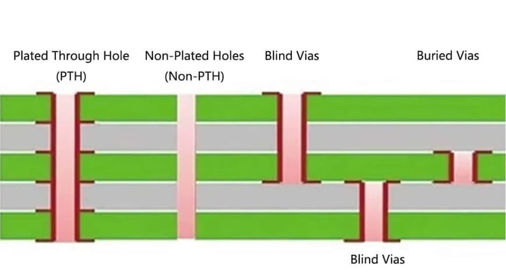
Vias in multilayer PCBs come in various forms, each with distinct characteristics suited to specific applications. The primary types include through-hole vias, blind vias, and buried vias. Through-hole vias extend through the entire board, connecting all layers. Blind vias connect an outer layer to an inner layer without penetrating the full board thickness. Buried vias, on the other hand, link internal layers and remain invisible from the board's surface.
The choice of via type impacts signal integrity and board layout. For instance, through-hole vias are simple to manufacture but consume more space, potentially interfering with routing on other layers. Blind vias and buried vias offer space-saving benefits, ideal for high-density designs, but require precise manufacturing processes to avoid defects. According to industry standards like IPC-2221B, Generic Standard on Printed Board Design, via dimensions and placement must account for current carrying capacity and thermal expansion to prevent failures.
Via design also involves considerations of aspect ratio, which is the ratio of via depth to diameter. A high aspect ratio can complicate plating and increase the risk of defects. Standards such as IPC-6012E recommend maintaining aspect ratios within acceptable limits to ensure reliable connections. Engineers must balance these technical constraints with the electrical demands of their designs to achieve optimal performance.
Suggested Reading: FR 4 PCB Vias: Types, Design Rules, and Manufacturing Considerations
Factors Influencing PCB Via Selection
Selecting the right via for multilayer PCB designs requires evaluating multiple factors. First, consider the layer count and board thickness. High layer counts often necessitate blind vias or buried vias to manage routing density without overcrowding surface layers. Board thickness impacts via drilling and plating, influencing the choice of via type based on manufacturing capabilities.
Signal integrity is another critical factor in PCB via selection. High-speed signals are sensitive to impedance mismatches caused by vias. Minimizing via stub length, especially in through-hole designs, helps reduce signal reflections. For high-frequency applications, buried vias can be preferable as they avoid stubs entirely by remaining within internal layers.
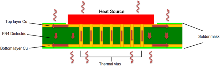
Thermal management also plays a role in via design. Vias can act as thermal conduits, dissipating heat from components to inner layers or heat sinks. Thermal vias, often placed under power components, must be sized according to current load and heat dissipation needs, as outlined in IPC-2152, Standard for Determining Current Carrying Capacity in Printed Board Design.
Finally, manufacturability and cost must be assessed. Blind vias and buried vias, while advantageous for dense layouts, increase fabrication complexity and cost due to sequential lamination processes. Through-hole vias are more cost-effective but less suitable for compact designs. Engineers must weigh these trade-offs to align with project budgets and timelines.
Practical Solutions for Via Design in Multilayer PCBs
Effective via design starts with defining clear requirements based on the application. For multilayer PCB vias, begin by mapping signal paths and power distribution needs across layers. This helps identify where vias are necessary and which type best suits each connection. Tools adhering to industry guidelines can assist in simulating signal performance to predict via impacts before fabrication.
When implementing blind vias, ensure drilling depth is controlled precisely to avoid penetrating unintended layers. IPC-2221B advises maintaining a minimum clearance between via walls and adjacent conductive features to prevent shorts. Collaboration with fabrication teams early in the design phase can clarify achievable tolerances and aspect ratios for reliable outcomes.
Buried vias, used in internal layer connections, require careful stack-up planning. Sequential lamination, where layers are built and pressed in stages, is often necessary. This process, while effective for hiding vias, demands strict adherence to standards like IPC-6012E to ensure interlayer alignment and plating quality. Engineers should specify via sizes and pad dimensions to match manufacturing capabilities.
For high-speed designs, consider via stub mitigation techniques. Back-drilling, a process to remove unused via portions, can minimize signal reflections in through-hole vias. Alternatively, using blind vias or buried vias eliminates stubs naturally. Ensure via placement avoids critical signal paths, maintaining consistent impedance as per design rules.
Thermal vias require strategic placement under heat-generating components. Grouping multiple small vias can enhance heat transfer while preserving structural integrity. Standards like IPC-2152 provide guidance on via count and spacing based on thermal load, ensuring effective dissipation without compromising board strength.
Best Practices for PCB Via Selection
To streamline PCB via selection, follow these best practices tailored for multilayer designs. Start with a thorough analysis of layer requirements to determine via distribution. Prioritize through-hole vias for simpler boards with fewer layers to keep costs low. Reserve blind vias and buried vias for high-density interconnects where surface space is limited.
Adhere to aspect ratio limits during via design. A ratio of 8:1 or lower, as suggested by IPC-6012E, ensures reliable plating and reduces defect risks. Specify via diameters based on current needs, using guidelines from IPC-2152 to prevent overheating or voltage drops in power connections.
Incorporate design for manufacturability principles. Consult fabrication guidelines to confirm minimum drill sizes and annular ring requirements for each via type. For blind vias and buried vias, verify lamination sequences to avoid misalignment. Clear documentation of via specifications aids in preventing errors during production.
Regularly review via placement for signal integrity. Position vias away from high-speed traces unless necessary, and use ground planes to shield signals. Simulate via effects on impedance to adjust layouts proactively. Following standards like IPC-2221B ensures designs meet performance and reliability criteria.
Conclusion
Selecting the right vias for multilayer PCB designs is a critical task that influences both performance and manufacturability. By understanding the distinct roles of through-hole, blind vias, and buried vias, engineers can tailor their via design to meet specific project needs. Balancing factors like signal integrity, thermal management, and cost requires a methodical approach grounded in industry standards. Practical solutions, such as precise drilling control and stub mitigation, enhance design outcomes in complex layouts. Adhering to best practices ensures that multilayer PCB vias contribute to reliable, high-performing boards. This guide serves as a foundation for informed PCB via selection, empowering engineers to tackle the challenges of modern electronics with confidence.
FAQs
Q1: What factors should influence PCB via selection for multilayer designs?
A1: PCB via selection hinges on layer count, signal integrity, and thermal needs. Consider board thickness and manufacturing constraints as well. High-density designs often require blind vias or buried vias to save space, while simpler boards can use through-hole vias for cost efficiency. Standards like IPC-2221B provide guidance on placement and sizing for optimal performance.
Q2: How do blind vias differ from buried vias in multilayer PCB vias?
A2: Blind vias connect an outer layer to an inner layer, visible only on one side. Buried vias link internal layers and are hidden from both surfaces. Both save space in via design, but buried vias require more complex lamination. IPC-6012E outlines manufacturing tolerances for ensuring reliability in these via types.
Q3: Why is via design critical for high-speed multilayer PCB applications?
A3: Via design affects signal integrity in high-speed applications by influencing impedance and reflections. Poorly placed multilayer PCB vias can cause signal distortion. Techniques like back-drilling or using blind vias reduce stubs. Following IPC-2152 ensures vias handle current without compromising performance in critical circuits.
Q4: What are the cost implications of using blind vias in PCB layouts?
A4: Blind vias increase fabrication costs due to precise drilling and sequential lamination processes. They are ideal for dense multilayer PCB vias but require strict adherence to standards like IPC-2221B for manufacturability. Weighing space savings against budget constraints is essential before integrating them into designs.
References
IPC-2221B — Generic Standard on Printed Board Design. IPC, 2012.
IPC-6012E — Qualification and Performance Specification for Rigid Printed Boards. IPC, 2020.
IPC-2152 — Standard for Determining Current Carrying Capacity in Printed Board Design. IPC, 2009.


