Introduction
In the realm of high-performance PCBs, signal integrity challenges arise as data rates climb into the multi-gigabit per second range. Traditional through-hole vias introduce stubs that create impedance discontinuities, leading to signal reflections and degradation. Advanced backdrilling techniques address this by selectively removing these stubs, enabling cleaner signal transmission across multiple layers. PCB stackup optimization plays a crucial role here, as the arrangement of layers directly influences via performance and overall board reliability. Engineers must consider layer stack considerations carefully to balance electrical performance with mechanical stability. This article explores how to integrate backdrilling into high-performance PCB designs for optimal results.
High-performance PCBs demand precise control over via structures to support protocols like PCIe and Ethernet at high speeds. Without proper backdrilling depth control, stubs longer than a fraction of the signal wavelength can attenuate signals significantly. Optimizing the stackup ensures that backdrilled vias align with active layers, minimizing parasitic effects. Manufacturers achieve this through controlled depth drilling, followed by plating removal. The result is improved insertion loss and return loss metrics essential for modern electronics. By mastering these elements, designers can push the boundaries of PCB capabilities.
What Is Backdrilling and Why It Matters for High-Performance PCBs
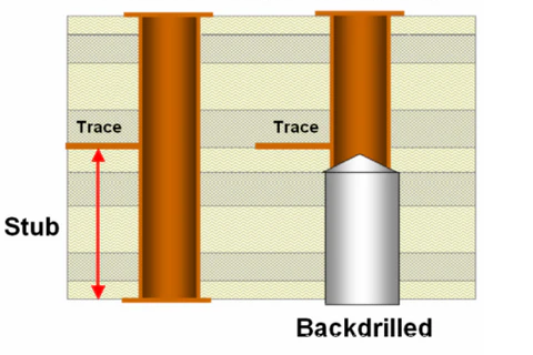
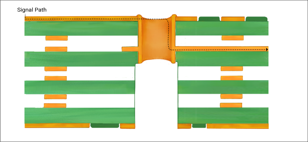
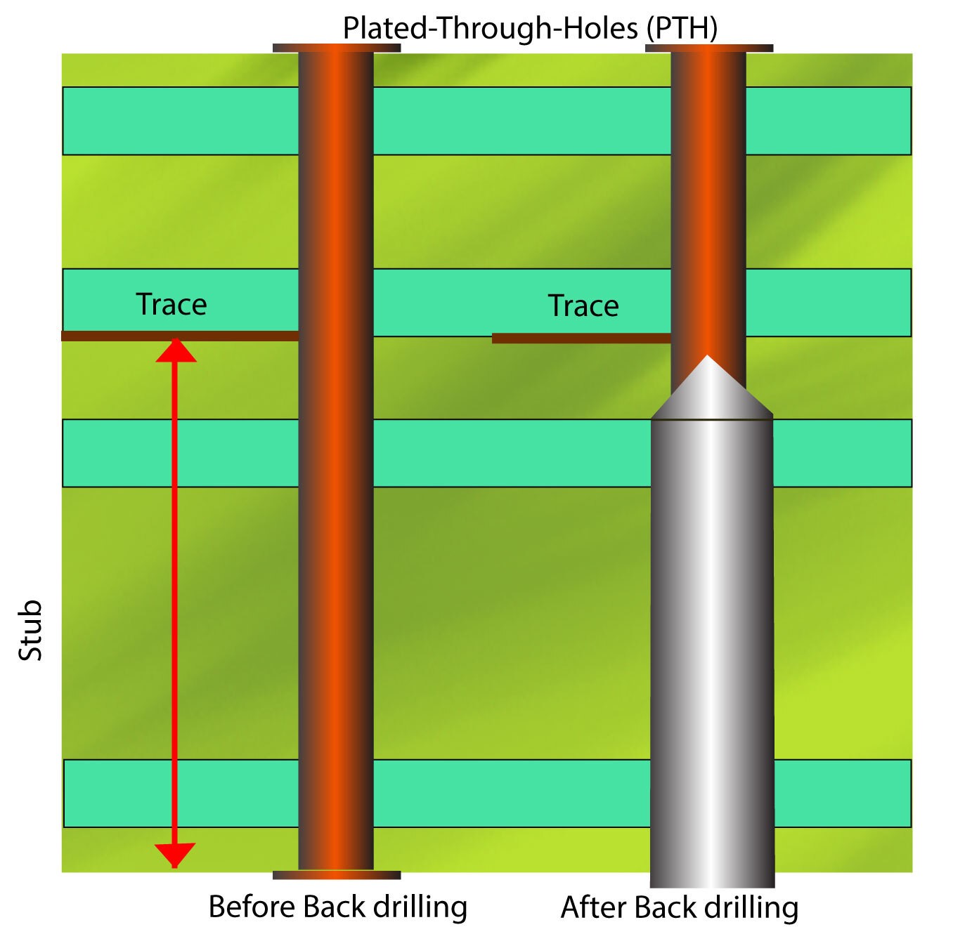
Backdrilling, also known as controlled depth drilling, involves drilling from the opposite side of a plated through-hole via to remove the unused copper barrel portion, or stub. This stub extends beyond the last connected layer, acting as a resonant transmission line that disrupts high-frequency signals. In high-performance PCBs, where rise times are sub-nanosecond, even short stubs introduce unacceptable reflections. Backdrilling shortens the effective via length, aligning it closely with the interconnect path and preserving signal quality.
The relevance of backdrilling intensifies with increasing layer counts and data rates. For instance, in stackups exceeding 20 layers, through-vias traverse numerous dielectrics, amplifying stub effects. Without intervention, crosstalk and eye diagram closure compromise system margins. PCB stackup optimization mitigates this by strategically placing signal layers and reference planes to reduce stub lengths inherently, but backdrilling provides the fine-tuned solution. Industry demands for high-performance PCBs in servers, telecom, and AI hardware make these techniques indispensable. Engineers prioritizing layer stack considerations ensure compliance with performance targets from the design phase.
Advanced backdrilling techniques further enhance outcomes by allowing multiple depths within the same board. This flexibility supports complex routing where vias serve different layer pairs. Depth control precision determines stub remnant, directly impacting impedance continuity. Poor control risks over-drilling into active layers, causing opens, while under-drilling leaves excessive stub. Thus, backdrilling elevates high-performance PCB designs from adequate to exceptional.
Technical Principles of Backdrilling and Stackup Interactions
The core principle of backdrilling revolves around via stub capacitance and inductance. A typical through-via in a multilayer stackup connects all layers, but signals only use a subset, leaving a stub that couples electromagnetically. This creates a low-impedance path at certain frequencies, causing reflections quantified by time-domain reflectometry. Backdrilling employs a larger diameter drill bit to excise the stub precisely, leaving a clean shoulder at the target depth. The process preserves plating on functional segments while eliminating parasitics.
PCB stackup optimization influences backdrilling efficacy through dielectric thickness and material properties. Thinner cores between signal layers shorten natural stub lengths, reducing backdrill dependency. Symmetric stackups around the neutral axis minimize warpage during fabrication, ensuring depth accuracy. Layer stack considerations include pairing high-speed signals with adjacent planes for return paths, optimizing impedance profiles. Material coefficient of thermal expansion matching prevents via barrel cracking under thermal stress. Engineers model these interactions using field solvers to predict post-backdrill performance.
Backdrilling depth control relies on mechanical drilling parameters like feed rate, spindle speed, and entry board materials. Depth stops and optical alignment systems maintain tolerances during production. Post-drill inspection via cross-sectioning verifies remnant stub lengths. IPC-6012E outlines qualification requirements for such features in rigid printed boards, emphasizing plating integrity and hole wall quality. These principles ensure vias behave as near-ideal interconnects in high-performance environments.
Signal propagation in backdrilled vias follows transmission line theory, where stub removal extends the usable bandwidth. Without backdrilling, the via's discontinuity scatters energy, degrading insertion loss by several dB at GHz frequencies. Optimized stackups incorporate blind or buried vias where possible, reserving backdrilling for cost-effective through-vias. Advanced techniques involve stepped backdrilling for multiple depths, demanding precise panel-level control. Layer transitions must account for drill breakout geometry to avoid damaging adjacent traces.
Related Reading: Backdrilling Design: A Beginner's Guide to Reducing Signal Reflections in PCBs
Practical Solutions and Best Practices for Implementation
Designers initiate PCB stackup optimization by defining signal layer assignments based on routing density and speed requirements. Place critical high-speed nets on outer layers or those with short stub potentials to minimize backdrill needs. Specify backdrill depths in fabrication notes, indicating target layers and oversize drill diameters, typically 10-20% larger than the via to ensure clean removal. Simulate via models pre- and post-backdrill to validate impedance steps. Layer stack considerations prioritize uniform core thicknesses for consistent drill depths across the panel.
During layout, group vias by backdrill depth to streamline manufacturing, using net classes for automation. Incorporate test coupons on panels for depth verification, including cross-section samples per IPC guidelines. Select materials with low loss tangents for high-performance layers adjacent to backdrilled vias. Fabrication partners confirm capabilities for depth tolerances suited to board thickness. Advanced backdrilling techniques benefit from sequential drilling sequences to avoid misalignment in asymmetric stackups.
Backdrilling depth control improves with entry and backup materials that reduce burrs and resin smear. Post-drill desmear ensures plating adhesion on remaining barrel. Electrical testing post-plating confirms continuity without shorts from incomplete stub removal. For high-performance PCBs, combine backdrilling with fine-line routing and fill stitching for ground integrity. Regular design reviews align stackup choices with manufacturability.
Best practices extend to reliability testing under thermal cycling, as backdrilled shoulders experience stress concentrations. IPC-2221B provides design guidelines for via reliability, stressing annular ring adequacy post-backdrill. Optimize plane cutouts around backdrill sites to prevent resonance. Documentation clarity prevents errors, specifying depths from reference sides. These steps yield robust high-performance PCBs ready for assembly.
Related Reading: Simulating Backdrilling: How to Optimize PCB Performance Before Manufacturing
Troubleshooting Common Challenges in Backdrilled Stackups
Depth inaccuracies top backdrilling issues, often from drill wander in thick stackups. Verify machine repeatability and use pilot holes for guidance. Over-drilling risks functional layer damage, detectable via flying probe tests showing opens. Under-drilling leaves stubs, confirmed by time-domain reflectometry exhibiting reflections. Cross-section analysis at multiple locations reveals variations tied to panel warpage.
Warpage in asymmetric layer stacks exacerbates depth control, pulling drill bits off-axis. Balance copper distribution and employ constraint cores. Plating voids at shoulders arise from inadequate desmear; enhance plasma cleaning. Signal integrity persists if remnant stubs exceed electrical budgets, necessitating resimulations. IPC-A-600K defines acceptability criteria for hole walls and shoulders, guiding inspections.
Reliability failures manifest as via cracks after reflow, linked to CTE mismatch. Select low-CTE materials for inner layers. Troubleshooting involves failure analysis via dye penetrant or scanning electron microscopy. Iterative stackup refinements resolve most issues preemptively.
Conclusion
Advanced backdrilling design transforms high-performance PCBs by eliminating via stubs that plague signal integrity. PCB stackup optimization and precise backdrilling depth control form the foundation, ensuring minimal discontinuities across complex layer stacks. Layer stack considerations like symmetry and material selection amplify these benefits, supporting ever-higher data rates. Practical implementation through simulation, clear specs, and verification upholds reliability standards. Engineers adopting these techniques achieve superior electrical performance without excessive cost. Future designs will lean further on such optimizations as speeds escalate.
FAQs
Q1: What role does PCB stackup optimization play in advanced backdrilling techniques?
A1: PCB stackup optimization positions signal layers to minimize stub lengths, reducing backdrill complexity. Symmetric arrangements control warpage, aiding depth accuracy. Reference planes adjacent to signals enhance return paths post-backdrill. This logical approach ensures high-performance PCB viability across layer counts.
Q2: How does backdrilling depth control impact high-performance PCB signal integrity?
A2: Precise backdrilling depth control removes stubs, preventing reflections that close eye diagrams. Tolerances dictate remnant length, directly affecting bandwidth. Verification via coupons confirms compliance. Layer stack considerations integrate this for optimal impedance continuity in high-speed nets.
Q3: Why are layer stack considerations critical for backdrilled high-performance PCBs?
A3: Layer stack considerations balance dielectric thicknesses and copper weights for uniform drilling. Matching CTE prevents stress at shoulders. Plane placement supports clean transitions. These factors sustain mechanical integrity alongside electrical gains from backdrilling.
Q4: When should engineers apply advanced backdrilling techniques in PCB design?
A4: Apply advanced backdrilling techniques when through-vias traverse unused layers in high-speed designs. Prioritize for data rates exceeding 10 Gbps where stubs degrade margins. Combine with stackup optimization for cost-effectiveness. Always simulate to quantify benefits.
References
IPC-6012E — Qualification and Performance Specification for Rigid Printed Boards. IPC, 2017
IPC-2221B — Generic Standard on Printed Board Design. IPC, 2012
IPC-A-600K — Acceptability of Printed Boards. IPC, 2020