Introduction
High-density interconnect (HDI) PCB design has become a cornerstone of modern electronics, enabling compact, high-performance devices. Multilayer PCB HDI structures support intricate routing and component density, critical for applications in telecommunications, medical devices, and consumer electronics. This article explores advanced HDI PCB design techniques, focusing on multilayer boards and the integration of microvias. By understanding these methods, electrical engineers can optimize signal integrity, reduce board size, and enhance reliability. The discussion will cover fundamental principles, best practices, and technical considerations aligned with industry standards. Whether designing for high-speed applications or space-constrained systems, mastering high-density interconnect techniques is essential for staying competitive in the fast-evolving electronics landscape. Let’s dive into the specifics of HDI PCB design for multilayer configurations.
What Is HDI PCB Design and Why It Matters
HDI PCB design refers to the use of high-density interconnect technology to create printed circuit boards with finer lines, smaller vias, and denser component placement. Unlike traditional PCBs, HDI boards incorporate microvias, blind vias, and buried vias to achieve higher routing density within multilayer structures. This approach is vital for modern electronics where miniaturization and performance are key drivers. Multilayer PCB HDI designs often include six or more layers, allowing complex circuitry in a reduced footprint.
The significance of high-density interconnect lies in its ability to support advanced applications. Smartphones, wearable devices, and automotive systems rely on HDI for efficient signal transmission and power distribution. By minimizing signal loss and crosstalk, HDI PCB design ensures reliability in high-speed environments. For engineers, adopting these techniques addresses challenges of space constraints while meeting stringent performance requirements.
Technical Principles of HDI PCB Design for Multilayer Boards
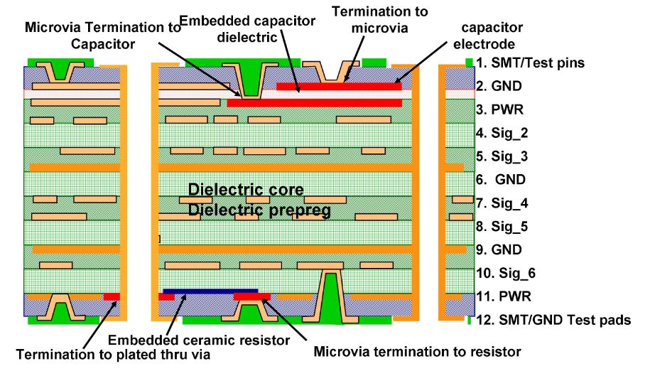
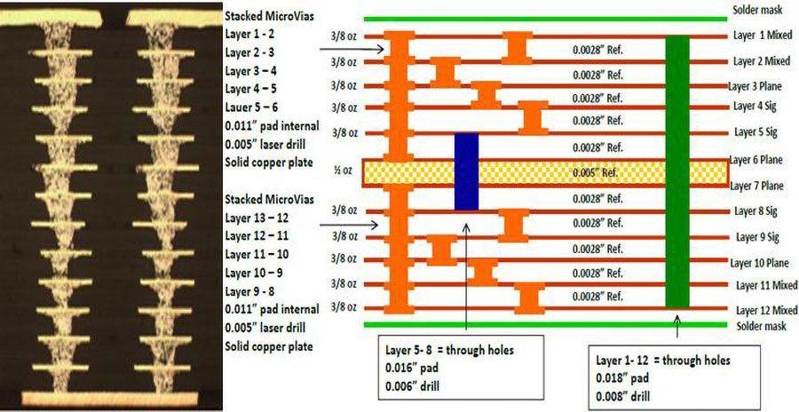
Understanding the core principles of multilayer PCB HDI design is crucial for effective implementation. At the heart of HDI technology are microvias, which are small-diameter vias typically less than 0.15 mm. These allow connections between layers without occupying excessive board space. Microvias can be laser-drilled for precision, enabling finer pitch components and tighter routing.
Another key element is the use of blind and buried vias. Blind vias connect an outer layer to an inner layer without penetrating the entire board, while buried vias link internal layers only. This structure maximizes routing space on outer layers for components. According to IPC-2226, a standard for HDI design, proper via placement and stack-up configuration are essential to maintain signal integrity and avoid manufacturing defects.
Layer stack-up planning is also critical in multilayer HDI boards. A balanced stack-up minimizes warpage and ensures uniform dielectric thickness. Engineers must consider impedance control, especially for high-speed signals, by selecting appropriate materials and layer arrangements. Ground planes should be strategically placed to reduce electromagnetic interference. These principles form the foundation for robust high-density interconnect designs.
Advanced PCB Design Techniques for Multilayer HDI Boards
Implementing advanced HDI PCB design techniques requires a focus on precision and adherence to best practices. Below are actionable strategies for optimizing multilayer PCB HDI layouts.
Optimizing Microvias in PCB Design
Microvias are indispensable in high-density interconnect boards. To ensure reliability, limit the aspect ratio of microvias to comply with IPC-6012E guidelines, which specify performance and qualification standards for rigid PCBs. Staggered or stacked microvias can be used to connect multiple layers, but alignment accuracy during fabrication must be verified. Laser-drilled microvias offer superior precision compared to mechanical drilling, reducing the risk of defects.
Via-in-Pad Design for Space Efficiency
Placing vias directly under component pads, known as via-in-pad, is a common technique in HDI PCB design. This method frees up routing space but requires careful planning to avoid solder wicking during assembly. Filling vias with conductive or non-conductive material, as recommended by IPC-A-600K for acceptability criteria, prevents voids and ensures proper soldering.
Signal Integrity and Impedance Control
High-speed applications demand strict control over signal integrity. Maintain consistent trace widths and spacing to achieve target impedance values. Use ground planes adjacent to signal layers to minimize crosstalk. Simulation tools aligned with industry practices can predict signal behavior in multilayer PCB HDI designs, allowing adjustments before fabrication.
Related Reading: Signal Integrity PCB Designers
Thermal Management Considerations
Dense component placement in HDI boards generates significant heat. Incorporate thermal vias to transfer heat to inner layers or heat sinks. Ensure that thermal vias are distributed evenly to avoid hotspots. Material selection, guided by standards like IPC-4101 for laminate specifications, plays a role in heat dissipation efficiency.
Layer Stack-Up Optimization
A well-designed stack-up reduces manufacturing complexity and enhances performance. Alternate signal and ground layers to shield high-speed traces. Follow IPC-2226 recommendations for HDI stack-up configurations to balance electrical and mechanical properties. This approach also aids in controlling board thickness and maintaining structural integrity.
Practical Best Practices for Multilayer HDI PCB Design
Beyond technical principles, practical best practices streamline the HDI PCB design process for multilayer boards. First, prioritize design for manufacturability. Consult fabrication capabilities early to align microvias PCB specifications with production limits. Aspect ratios, drill sizes, and layer counts must match manufacturer tolerances to avoid costly redesigns.
Second, adopt a systematic approach to component placement. Group related components to minimize trace lengths and reduce signal delay. Place high-speed components closer to connectors for efficient routing. This strategy enhances the effectiveness of high-density interconnect layouts.
Third, implement rigorous design rule checks. Automated tools can detect violations in trace spacing, via placement, and impedance mismatches. Cross-reference these checks with standards like IPC-2226 to ensure compliance. Thorough validation prevents errors from propagating to manufacturing stages.
Finally, consider testability during design. Include test points for critical nets to facilitate debugging and quality assurance. Ensure that test points are accessible without compromising the high-density layout. Following these practices leads to reliable multilayer PCB HDI designs that meet project goals.
Troubleshooting Common Challenges in HDI PCB Design
Multilayer HDI boards present unique challenges that engineers must address. One common issue is via reliability. Microvias can fail under thermal stress if not designed per IPC-6012E specifications. To mitigate this, use stacked microvias cautiously and verify plating quality during fabrication.
Another challenge is signal crosstalk in dense layouts. High-speed signals can interfere with adjacent traces if spacing is inadequate. Increasing separation or adding ground shielding resolves this issue. Refer to IPC-2221B for generic PCB design standards to guide trace routing.
Board warpage is also a concern in multilayer designs. Uneven layer distribution or improper material selection can cause deformation. Balance copper distribution across layers and select laminates per IPC-4101 guidelines to maintain flatness. Addressing these challenges ensures robust high-density interconnect performance.
Related Reading: HDI PCB Design: Overcoming Challenges in High-Density Interconnect
Conclusion
Mastering advanced HDI PCB design techniques for multilayer boards empowers engineers to create compact, high-performance electronics. By leveraging microvias, optimizing layer stack-ups, and adhering to industry standards like IPC-2226, designers can achieve reliable high-density interconnect solutions. Practical strategies, such as via-in-pad implementation and signal integrity control, further enhance design outcomes. Overcoming challenges like via reliability and crosstalk requires meticulous planning and validation. For electrical engineers, these methods are indispensable in meeting the demands of modern applications. Implementing these insights ensures that multilayer PCB HDI designs deliver both functionality and durability in competitive markets.
FAQs
Q1: What are the key benefits of HDI PCB design for multilayer boards?
A1: HDI PCB design offers significant advantages for multilayer boards, including reduced board size and enhanced signal integrity. It supports denser component placement through microvias and blind vias, ideal for compact devices. This approach also improves electrical performance by minimizing signal paths, making it essential for high-speed applications in electronics.
Q2: How do microvias improve multilayer PCB HDI performance?
A2: Microvias in PCB design enable finer connections between layers, allowing higher routing density in multilayer PCB HDI layouts. Their small size, often less than 0.15 mm, saves space and supports miniaturization. When designed per industry standards, microvias ensure reliable interlayer connectivity and enhance overall board performance.
Q3: What standards should guide high-density interconnect design practices?
A3: High-density interconnect designs must follow recognized standards like IPC-2226 for HDI-specific guidelines and IPC-6012E for performance specifications. These standards ensure manufacturability, reliability, and signal integrity. Adhering to them helps engineers avoid common pitfalls and achieve consistent quality in multilayer HDI boards.
Q4: How can signal integrity be maintained in multilayer HDI PCB layouts?
A4: Maintaining signal integrity in multilayer PCB HDI designs involves controlling impedance with consistent trace widths and strategic ground plane placement. Minimize crosstalk by spacing traces appropriately and shielding high-speed signals. Following guidelines from standards like IPC-2221B ensures effective routing and reduces interference in dense layouts.
References
IPC-2226 — Sectional Design Standard for High Density Interconnect (HDI) Printed Boards. IPC, 2003.
IPC-6012E — Qualification and Performance Specification for Rigid Printed Boards. IPC, 2020.
IPC-A-600K — Acceptability of Printed Boards. IPC, 2020.
IPC-2221B — Generic Standard on Printed Board Design. IPC, 2012.
IPC-4101E — Specification for Base Materials for Rigid and Multilayer Printed Boards. IPC, 2017.


