Introduction
High-frequency PCB designs push the boundaries of traditional routing methods, where signal speeds exceed gigahertz ranges and even minor layout errors can degrade performance. Electrical engineers face challenges like signal reflections, crosstalk, and attenuation that demand precise high-frequency PCB trace routing strategies. Advanced techniques such as controlled impedance routing and differential pair routing become essential to preserve waveform integrity across the board. These methods ensure reliable data transmission in applications ranging from telecommunications to radar systems. By mastering signal integrity routing principles, designers can mitigate losses and electromagnetic interference effectively. This article explores structured approaches to optimize routing for high-frequency environments.
The Critical Role of Routing in High-Frequency PCB Designs
In high-frequency PCB trace routing, signals behave as transmission lines rather than simple conductors, making routing topology a primary determinant of performance. Poor routing leads to impedance mismatches that cause reflections, distorting signals and reducing eye diagram margins. Industry relevance stems from the exponential growth in data rates, where even picosecond delays matter. Controlled impedance routing addresses these issues by maintaining consistent characteristic impedance along traces. Differential pair routing further enhances noise immunity, crucial for balanced signals in high-speed interfaces. Ultimately, effective signal integrity routing aligns with engineering goals of minimizing bit error rates and maximizing throughput.
Fundamentals of Transmission Line Theory for PCB Routing
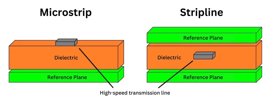
Transmission line theory underpins all high-frequency PCB designs, where the characteristic impedance depends on trace geometry, dielectric properties, and reference planes. Microstrip routing high-frequency signals places traces on outer layers adjacent to a ground plane, offering ease of fabrication but susceptibility to radiation losses. In contrast, stripline configurations embed traces between ground planes, providing better shielding at the cost of routing flexibility. Engineers must calculate impedance using stackup parameters to avoid discontinuities. According to IPC-2141A guidelines, controlled impedance design starts with precise modeling of these structures. Proper reference planes ensure return currents follow the shortest path, reducing inductance.
Implementing Controlled Impedance Routing
Controlled impedance routing requires a well-defined layer stackup with consistent dielectric thickness and low-loss materials to sustain target impedance values. Engineers select trace widths, spacings, and thicknesses based on field solver predictions or standard equations for microstrip and stripline geometries. Maintaining uniformity prevents step changes that introduce reflections, especially at via transitions or bends. High-frequency PCB trace routing benefits from solid ground or power planes as references, minimizing loop inductance. Fabrication tolerances must align with design margins to achieve the specified impedance tolerance, typically tight for multi-gigabit signals. This technique forms the foundation of signal integrity routing across all high-speed nets.
Mastering Differential Pair Routing Techniques
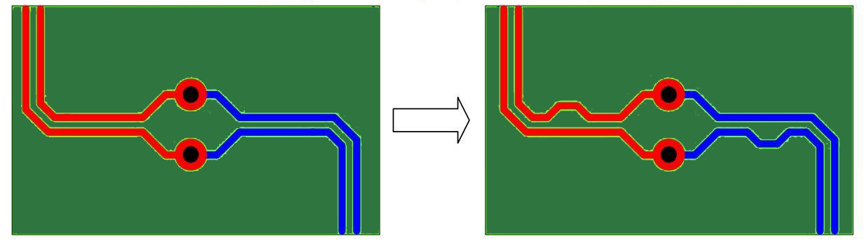
Differential pair routing transmits signals as complementary pairs, rejecting common-mode noise and enabling higher data rates in high-frequency designs. Key to success is maintaining equal trace lengths and constant intra-pair spacing to preserve differential impedance and phase alignment. Route pairs on the same layer with symmetric geometries, avoiding splits that alter coupling. When layer changes are necessary, use via pairs with identical stub lengths and back-drilling to eliminate stubs. Symmetry extends to bends, where serpentine or curved patterns equalize lengths without skew. IPC-2221 provides foundational spacing rules that support these practices in controlled environments.
Microstrip Routing Strategies for High-Frequency Applications
Microstrip routing high-frequency signals leverages outer-layer traces for accessibility, but demands careful crosstalk management due to exposed fields. Implement spacing rules like three times the trace width between adjacent signals to suppress near-end and far-end coupling. Continuous ground planes beneath traces stabilize impedance and provide low-impedance return paths. Avoid right-angle bends, opting for 45-degree mitered corners or smooth arcs to reduce reflections. In dense layouts, alternate signal directions on adjacent layers to minimize broadside coupling. These strategies enhance signal integrity routing while accommodating probe access for testing.
Advanced Best Practices for Signal Integrity Routing
Signal integrity routing begins with planning: assign high-speed nets to inner layers where possible, reserving outer layers for lower-speed signals. Minimize via count by optimizing component placement and using blind or buried vias judiciously. Length tuning ensures timing alignment for clock and data lines, preventing skew-induced errors. Employ guard traces or stitching vias along edges to contain EMI. For crosstalk mitigation, adhere to spacing guidelines and route sensitive pairs away from aggressors. Post-layout verification through simulation confirms compliance before fabrication.
- Maintain solid reference planes without splits under high-frequency traces.
- Use length-matched meanders for differential pairs exceeding critical lengths.
- Apply back-drilling to remove via stubs longer than one-tenth wavelength.
- Segregate analog and digital routing domains to prevent noise coupling.
Common Pitfalls and Troubleshooting in High-Frequency Routing
Engineers often overlook stackup variations during fabrication, leading to impedance drifts that manifest as eye closure. Vias introduce capacitance and inductance; clustering them exacerbates return path disruptions. Unequal ground plane stitching around pairs causes mode conversion, degrading common-mode rejection. Troubleshooting involves time-domain reflectometry to pinpoint discontinuities and adjusting spacings iteratively. Simulate fanout from high-pin-count devices early to preempt congestion. Adhering to IPC-6012E performance specs ensures fabricated boards meet design intent.
Conclusion
Advanced routing techniques transform high-frequency PCB designs from potential failure points into robust performers. Controlled impedance routing, differential pair routing, and microstrip routing high-frequency signals collectively safeguard against SI threats. Electrical engineers benefit from structured adherence to principles like symmetry, uniformity, and minimization of discontinuities. Integrating these with stackup optimization yields reliable, high-throughput boards. Future designs will demand even tighter margins, underscoring the value of proactive signal integrity routing. Mastery here elevates design quality across applications.
FAQs
Q1: What is controlled impedance routing in high-frequency PCB trace routing?
A1: Controlled impedance routing maintains a constant characteristic impedance along traces by precisely controlling width, thickness, spacing, and dielectric properties. This prevents reflections and distortion in high-speed signals. Engineers use stackup calculators aligned with standards like IPC-2141A to achieve tolerances under 10 percent. Proper implementation ensures clean signal propagation without termination adjustments.
Q2: How does differential pair routing improve signal integrity routing?
A2: Differential pair routing uses balanced traces to cancel common-mode noise, ideal for high-frequency environments. Maintain equal lengths and spacings for consistent differential impedance, typically around 100 ohms. Symmetric routing minimizes skew and EMI susceptibility. Avoid vias unless paired identically to preserve balance. This technique boosts eye height in multi-gigabit links.
Q3: Why choose microstrip routing high-frequency over stripline?
A3: Microstrip routing high-frequency offers surface access for tuning and probing, suiting RF front-ends. It uses outer layers with ground reference, but requires wider spacings for crosstalk control. Stripline provides superior shielding for digital signals. Select based on radiation tolerance and layer availability. Both demand controlled impedance for integrity.
Q4: What are key best practices for high-frequency PCB trace routing?
A4: Prioritize solid planes, minimize vias, and enforce spacing rules like 3W between traces. Length-match critical nets and miter bends to cut reflections. Verify with simulations pre-fabrication. Align with IPC-2221 for spacing and routing guidelines. These ensure robust signal integrity routing.
References
IPC-2141A — Design Guide for High-Speed Controlled Impedance Circuit Boards. IPC, 2004
IPC-2221B — Generic Standard on Printed Board Design. IPC, 2012
IPC-6012E — Qualification and Performance Specification for Rigid Printed Boards. IPC, 2017


