Introduction
Printed circuit board design forms the foundation of reliable electronic systems, yet even experienced electrical engineers encounter challenges that lead to costly revisions. A comprehensive PCB design review process systematically evaluates design files, schematics, and layouts to uncover issues early in the development cycle. This approach directly influences PCB design review cost by preventing expensive prototypes, manufacturing delays, and field failures. Engineers often overlook subtle interactions between layers, signals, and materials, which amplify expenses during production scaling. By adopting a structured PCB design review checklist, teams achieve cost reduction in PCB design without compromising performance. This guide outlines logical steps and engineering principles to conduct effective reviews, drawing on established practices for multilayer boards.
Understanding PCB Design Review
PCB design review involves a multi-stage examination of Gerber files, drill data, bill of materials, and assembly drawings against functional requirements and manufacturability constraints. Electrical engineers perform this review to verify compliance with electrical performance, mechanical integrity, and fabrication tolerances. The process typically includes peer checks, automated design rule verification, and simulation validations for signal and power integrity. Key outputs include annotated feedback reports and revised files ready for fabrication. Without this step, discrepancies between design intent and physical realization emerge, escalating PCB design review cost through iterations. A well-executed review aligns design with production capabilities, ensuring first-pass success.
Why PCB Design Review Matters in Cost Reduction
Overlooking design flaws translates to multiplied expenses at each production stage, from tooling to assembly rework. Early detection during review prevents scrap rates and yield losses that strain budgets, particularly for high-density interconnect boards. For instance, mismatched trace widths or via placements can cause signal degradation, necessitating respins that dwarf initial savings. Implementing a PCB design review checklist fosters proactive cost reduction in PCB design by quantifying risks like thermal hotspots or impedance mismatches. Industry experience shows that thorough reviews reduce overall project timelines by addressing issues upstream. Electrical engineers benefit from this discipline, as it safeguards intellectual property value and accelerates time-to-market.
Key Technical Areas for PCB Design Review
Layer Stackup and Material Selection
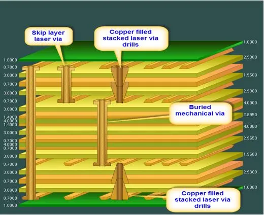
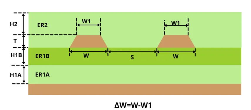
Layer stackup defines the electrical and mechanical backbone of the PCB, influencing impedance control and thermal dissipation. Engineers must verify core and prepreg thicknesses align with controlled impedance requirements for high-speed signals. Common errors include inadequate plane clearances or asymmetric builds that induce warpage during reflow. Review stackup diagrams for sequential lamination compatibility and material CTE matching to prevent delamination. Adherence to guidelines in IPC-2221B ensures balanced capacitance and minimal crosstalk between layers. Simulate the stackup response to fabrication tolerances to anticipate variations in board thickness.
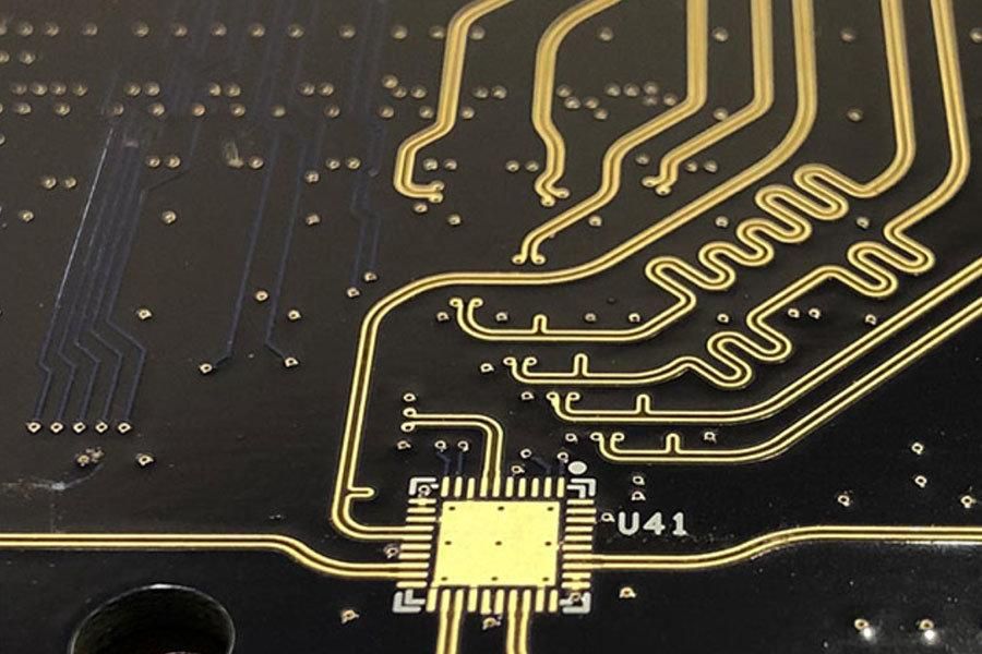
Routing and Signal Integrity
Trace routing demands precision to maintain signal fidelity, especially for gigabit interfaces where reflections degrade performance. Check for excessive vias in critical paths, which introduce stubs and attenuation. Verify length matching for clocks and data lines to avoid skew-induced timing violations. Electrical engineers should analyze return paths and ground plane splits that create inductive loops. Route reviews also confirm clearance rules prevent shorts under thermal expansion. Post-layout simulations validate eye diagrams and jitter budgets before committing to fabrication.
Power Distribution and Decoupling
Power integrity failures manifest as voltage droops during transient loads, compromising logic levels across the board. Distribute planes generously with stitching vias to minimize resistance and inductance in PDN. Place decoupling capacitors strategically near IC power pins, considering package parasitics and ESL. Review current carrying capacity using width calculators to avoid overheating narrow traces. Engineers must model simultaneous switching noise to ensure ripple stays within tolerances. This step in the PCB design review checklist directly contributes to reliable operation under full load.
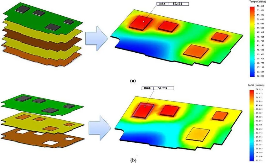
Thermal Management and Mechanical Integrity
Heat accumulation in dense layouts triggers reliability issues like solder joint fatigue. Assess via thermal resistance and copper pour effectiveness for hotspot mitigation. Verify pad sizes and thermal relief patterns comply with assembly processes to prevent tombstoning. Mechanical reviews examine board outline clearances, fiducials, and mounting hole tolerances for fixture compatibility. Simulate warpage from CTE mismatches between copper and substrate. Proper attention here avoids costly qualification failures in environmental testing.
Comprehensive PCB Design Review Checklist
A standardized PCB design review checklist streamlines inspections and minimizes oversights. Use this logical framework divided into categories for thorough coverage.
Schematic Verification:
- Confirm netlist matches between schematic and layout.
- Check component values, footprints, and polarity.
- Validate power sequencing and protection circuits.
- Ensure bypass capacitors align with frequency response needs.
Layout and Routing Checks:
- Measure trace widths against current and impedance specs.
- Confirm drill sizes and aspect ratios for vias.
- Inspect silkscreen legibility and polarity markers.
- Verify no acute angles in polygons that cause etching defects.
DFM/DFA Focus:
- Review annular ring sizes per fabrication capabilities.
- Check solder mask expansion and clearances.
- Confirm BGA fanout with dogbone vias if required.
- Assess panelization rails and tooling tabs.
Documentation Review:
- Ensure fab and assembly notes specify finishes and tolerances.
- Validate BOM completeness with sourcing notes.
- Cross-check ODB++ or Gerber panel files.
Integrating this checklist into workflows drives cost reduction in PCB design by catching 80-90% of issues pre-fab, based on engineering discipline.
Best Practices for Conducting PCB Design Reviews
Assign cross-functional teams including design, manufacturing, and test engineers for diverse perspectives. Schedule reviews at 60% and 95% layout completion to balance progress and iteration time. Leverage automated DRC tools alongside manual inspections for hybrid validation. Document findings in a centralized tracker with severity ratings and resolution plans. For complex boards, perform electromagnetic simulations to quantify EMI risks. Revisit past review lessons to refine the PCB design review checklist iteratively. These practices not only lower PCB design review cost but enhance team expertise over projects.
Incorporate IPC-A-600K criteria during visual checks to align with acceptability standards for conductor definition and plating. Separate signal and power reviews to avoid cognitive overload. Prototype small panels for empirical validation where simulations fall short. Foster a blame-free culture to encourage candid feedback. Track metrics like defect escape rate to measure review efficacy.
Troubleshooting Common Pitfalls
Engineers frequently encounter impedance drift from unaccounted copper weight variations. Mitigate by specifying foil thickness explicitly in notes. Another pitfall involves blind via transitions overlooked in stackups, leading to open circuits. Always plot sequential cross-sections to visualize transitions. Ground bounce from insufficient decoupling plagues digital designs; counter with PDN impedance plots under load. Fabricators flag undersized pads causing paste starvation in SMT. Scale pads conservatively and simulate stencil apertures.
Conclusion
Mastering PCB design review transforms potential pitfalls into strengths, delivering robust boards on budget. A disciplined PCB design review checklist, coupled with deep technical scrutiny, yields measurable cost reduction in PCB design. Electrical engineers who prioritize stackup integrity, signal routing, power distribution, and DFM set projects up for success. Regular application of these principles minimizes respins and accelerates innovation. Commit to structured reviews as a core workflow to avoid costly mistakes and elevate design quality.
FAQs
Q1: What should a PCB design review checklist include?
A1: A comprehensive PCB design review checklist covers schematic netlist integrity, layer stackup verification, trace routing for impedance control, power plane distribution, thermal via placement, and DFM elements like annular rings and fiducials. Electrical engineers prioritize signal integrity simulations and mechanical tolerances to prevent fabrication issues. This structured approach ensures alignment with performance specs and reduces PCB design review cost through early detection. Tailor it to board complexity for optimal results.
Q2: How does PCB design review contribute to cost reduction in PCB design?
A2: PCB design review identifies errors like via misalignment or inadequate clearances before prototyping, avoiding scrap and rework expenses. By validating against standards such as IPC-2221B, teams eliminate yield killers that inflate production costs. Engineers save on iterations, enabling faster scaling and resource allocation to innovation. Proactive checklists minimize delays, directly lowering overall PCB design review cost while maintaining reliability.
Q3: What are common mistakes in PCB design review?
A3: Overlooking asymmetric stackups leads to warpage, while ignoring return path continuity causes EMI. Engineers often miss decoupling placement nuances, resulting in voltage droops. Neglecting fab notes on surface finishes invites assembly defects. Use layered checklists and simulations to catch these, ensuring cost reduction in PCB design. Peer involvement adds diverse insights for thorough coverage.
Q4: Why is signal integrity critical in PCB design review?
A4: Signal integrity review prevents crosstalk, reflections, and timing skew in high-speed designs through controlled impedance traces and length matching. Electrical engineers analyze eye patterns and TDR measurements to confirm margins. This step averts functional failures post-assembly, tying into broader PCB design review cost savings. Compliance with routing guidelines sustains data rates across interfaces.
References
IPC-2221B — Generic Standard on Printed Board Design. IPC, 2003
IPC-A-600K — Acceptability of Printed Boards. IPC, 2020
IPC-6012E — Qualification and Performance Specification for Rigid Printed Boards. IPC, 2017