Introduction
High speed design in printed circuit boards demands precise control over signal paths to prevent degradation. Vias serve as essential interconnects between layers, but traditional through-hole vias create stubs that disrupt signal propagation. Backdrilling and blind vias address this by enabling via stub reduction, which leads to signal integrity improvement. Engineers benefit from combining these techniques to maintain controlled impedance across multilayer stackups. This approach proves vital for applications operating at multi-gigabit rates, where reflections can cause failures. By understanding their mechanisms, designers can optimize performance without excessive complexity.
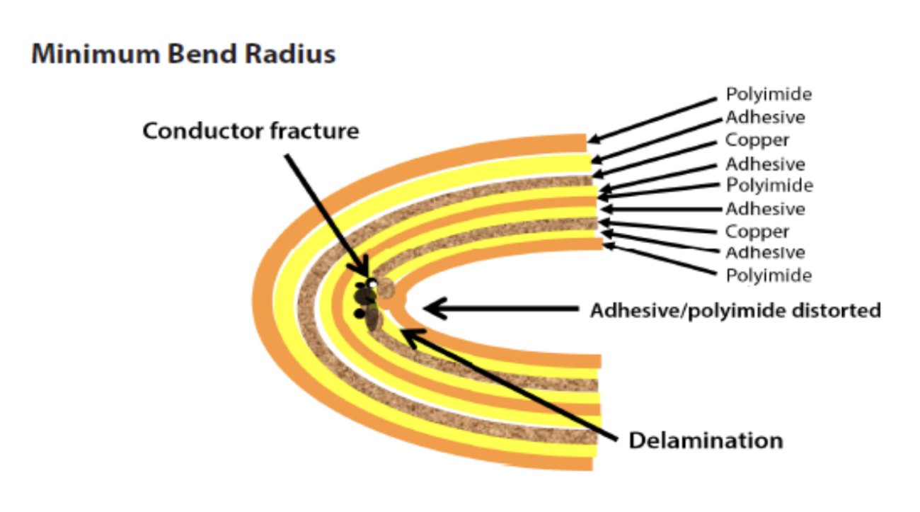
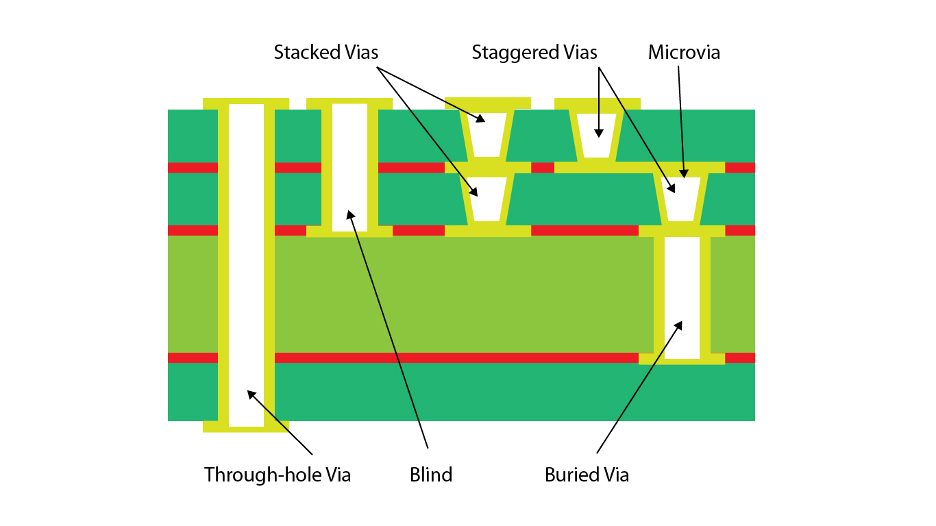
The Role of Vias in Multilayer PCBs
Vias facilitate vertical routing in multilayer boards, connecting traces across dielectric layers. In standard through-hole vias, plating extends fully from top to bottom, leaving unused segments known as stubs. These stubs function as open-ended transmission lines, generating reflections at frequencies where their electrical length matches signal harmonics. Signal integrity suffers through increased insertion loss, crosstalk, and jitter. High speed design requires strategies like backdrilling blind via implementations to mitigate these effects. Controlled impedance preservation becomes feasible only with minimal discontinuities.
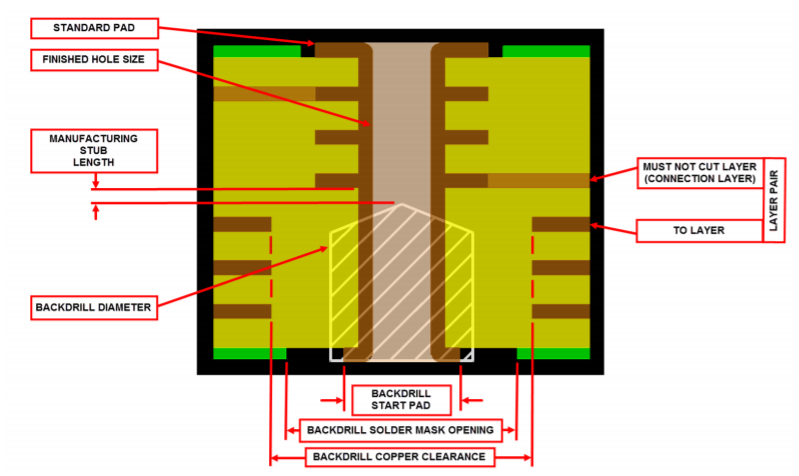
Defining Backdrilling for Via Stub Reduction
Backdrilling removes the non-functional stub portion of a through-via by drilling a slightly larger hole from the opposite board side after initial plating. This controlled depth drilling targets the copper barrel precisely, leaving the required interconnection intact. The process demands accurate depth control to avoid damaging adjacent nets or layers. Manufacturers verify stub removal through cross-section analysis or electrical testing. IPC-2221B outlines design parameters for vias intended for backdrilling, emphasizing annular ring margins and drill size differences. This technique excels in deeper stackups where full blind vias prove impractical.
Related Reading: Simulating Backdrilling: How to Optimize PCB Performance Before Manufacturing
Blind Vias: Precision Interconnects Without Full Penetration
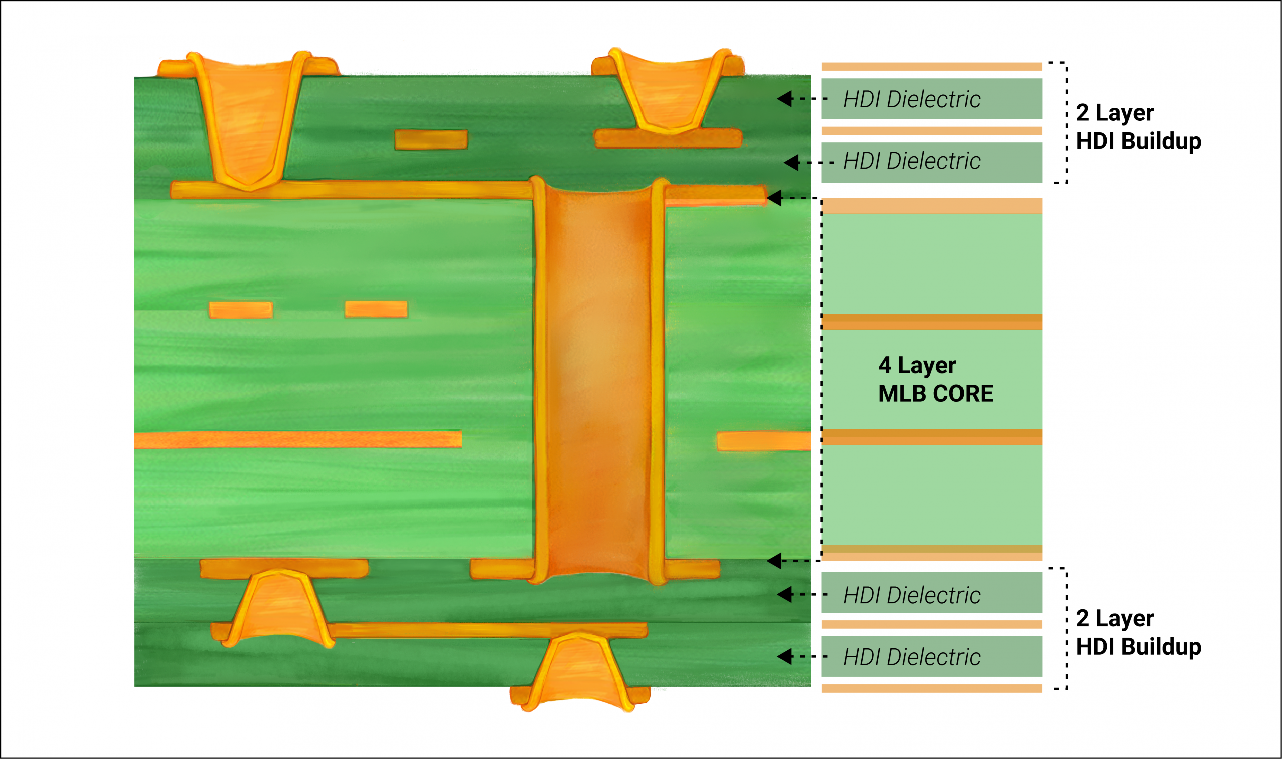
Blind vias link an outer layer to one or more inner layers without traversing the entire board thickness. Fabricated via sequential build-up or laser drilling, they inherently limit stub length to the targeted depth. This reduces parasitic effects compared to through-vias, supporting denser routing. In high speed design, blind vias maintain smoother impedance transitions for surface-layer signals. Combining them with buried vias further optimizes inner-layer connectivity. Their use aligns with requirements for signal integrity improvement in compact assemblies.
Why Combine Backdrilling and Blind Vias?
A backdrilling blind via strategy leverages the strengths of both methods for comprehensive coverage. Blind vias handle short-reach outer transitions efficiently, while backdrilling cleans up stubs in longer through-vias deeper in the stackup. This hybrid reduces overall via capacitance and inductance across all nets. Signal paths exhibit fewer reflections, enhancing eye quality and bit error rates. Controlled impedance profiles remain consistent, crucial for differential pairs in high speed design. The combination minimizes layer count needs, balancing cost and density.
Related Reading: Advanced Backdrilling Design: Optimizing Stackup for High Performance PCBs
Technical Mechanisms of Signal Integrity Improvement
Via stubs introduce impedance mismatches due to their higher inductance relative to trace segments. At high frequencies, signals reflect at the stub end, interfering with incoming waves. Backdrilling shortens stubs to wavelengths far below signal rise times, effectively making them transparent. Blind vias eliminate stubs entirely for their span, preserving return currents close to signal paths. Together, they reduce crosstalk coupling and ground bounce. Simulations confirm these changes yield flatter insertion loss curves and stable controlled impedance.
Impact on Controlled Impedance in High Speed Design
Controlled impedance relies on uniform transmission line characteristics throughout the signal path. Vias disrupt this with antipad clearances and stub parasitics. Backdrilling aligns via impedance closer to trace values by removing excess barrel. Blind vias allow tighter antipads, fine-tuning differential impedance. Engineers calculate effective lengths considering dielectric constants and plating thickness. This ensures compliance with stackup targets, vital for multi-gigabit signaling.
Best Practices for Implementation
Start with stackup planning to assign high-speed nets to layers minimizing via depth. Specify backdrill depths with 0.1 mm tolerances, accounting for drill wander. Use larger drill sizes for backdrills to ensure clean stub removal without residue. IPC-6012E defines acceptance criteria for backdrilled hole walls and plating integrity. Integrate blind vias for peripherals, reserving backdrilling for core routing. Prototype testing via vector network analysis validates signal integrity improvement.
- Stub Reduction: Backdrilling — Removes inner stubs; Blind Vias — Eliminates outer stubs; Combined Approach — Full stackup coverage.
- Cost Impact: Backdrilling — Moderate increase; Blind Vias — Higher due to lamination; Combined Approach — Optimized balance.
- Density Benefit: Backdrilling — Good for deep layers; Blind Vias — Excellent for surfaces; Combined Approach — Maximizes routing.
- Fabrication Complexity: Backdrilling — Depth control; Blind Vias — Sequential build; Combined Approach — Managed hybrid.
Overcoming Common Challenges
Fabrication tolerances challenge backdrilling alignment, risking net shorts if overshoot occurs. Blind vias demand precise laser registration for microvia fills. Cost escalates with added steps, so reserve for critical nets exceeding 3 Gbps. Design rules must include spacing between backdrill sites to prevent interaction. Material warpage during lamination affects depth accuracy in thick boards. Solutions involve symmetric stackups and fixture-based drilling.
Practical Insights for Electric Engineers
Engineers prioritize via farms near connectors, applying backdrilling to fanout vias. Differential pairs benefit from matched blind via pairs for symmetry. Simulate stub resonance frequencies early to justify techniques. Collaborate with fabricators on drill charts specifying sizes and depths. Monitor plating uniformity, as thin walls amplify losses. This structured approach ensures robust high speed design outcomes.
Conclusion
Backdrilling and blind vias form a synergistic pair for tackling via stub reduction in demanding applications. Their combined use delivers signal integrity improvement through minimized reflections and stable controlled impedance. High speed design thrives on such precise interventions, aligning with multilayer complexity trends. Adhering to standards like IPC guidelines guarantees reliability. Designers achieve optimal performance by thoughtfully selecting and implementing these methods.
FAQs
Q1: What is a backdrilling blind via, and how does it aid via stub reduction?
A1: A backdrilling blind via integrates blind via construction with post-plating stub removal from the blind end. This hybrid targets residual stubs in semi-penetrating vias, ensuring complete elimination. It proves effective in high speed design where partial blind vias leave minor discontinuities. The result is smoother signal paths with reduced reflections, enhancing overall board performance. Engineers specify it for transitional layers in dense stackups.
Q2: How does backdrilling contribute to signal integrity improvement in high speed PCBs?
A2: Backdrilling shortens through-via stubs to negligible lengths, preventing resonant reflections that degrade high-frequency signals. This maintains signal amplitude and timing margins critical for multi-gigabit rates. Combined with proper antipad sizing, it preserves controlled impedance profiles. Testing shows cleaner eye diagrams post-implementation. Limit its use to nets requiring stringent integrity to manage costs.
Q3: Why use blind vias alongside backdrilling for controlled impedance?
A3: Blind vias provide stub-free transitions for outer layers, complementing backdrilling's inner cleanup. Together, they uniformize impedance across the stackup, vital for differential signaling. This avoids capacitance spikes from long barrels. Design stackups to leverage both for optimal reference plane proximity. The approach supports higher densities without performance trade-offs.
Q4: When should engineers prioritize backdrilling blind via in high speed design?
A4: Prioritize in boards over 10 layers with signals above 5 Gbps, where through-stubs dominate losses. Assess via depths against rise time budgets first. Blind vias suffice for shallow nets, reserving backdrilling for deeper ones. Verify via simulation tools for justification. This ensures cost-effective signal integrity improvement.
References
IPC-2221B — Generic Standard on Printed Board Design. IPC, 2009
IPC-6012E — Qualification and Performance Specification for Rigid Printed Boards. IPC, 2017
IPC-A-600K — Acceptability of Printed Boards. IPC, 2020