Introduction
As electronic hobbyists dive deeper into PCB design basics, they often encounter challenges with signal integrity in faster circuits. Devices like microcontrollers running at higher clock speeds or interfaces such as USB 3.0 demand cleaner signal paths to avoid errors and glitches. One common culprit is signal reflections caused by via stubs in multilayer boards. PCB backdrilling for beginners offers a straightforward solution to mitigate these issues without advanced fabrication techniques. This guide breaks down the concepts, principles, and steps in a logical way, helping you understand via stub effects and implement basic backdrilling techniques effectively. By the end, you’ll see how signal reflection reduction fits into your next project.
Backdrilling removes the unused portion of a through-hole via, creating a shorter path for high-speed signals. Hobbyists prototyping with 4–8 layer boards will find this technique accessible once they grasp the fundamentals. It aligns with standard PCB manufacturing practices, ensuring reliable performance without excessive costs.
What Is Backdrilling and Why It Matters
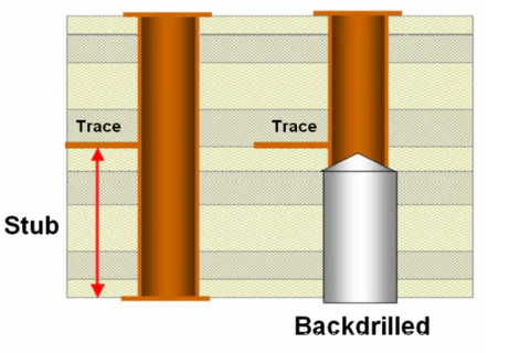
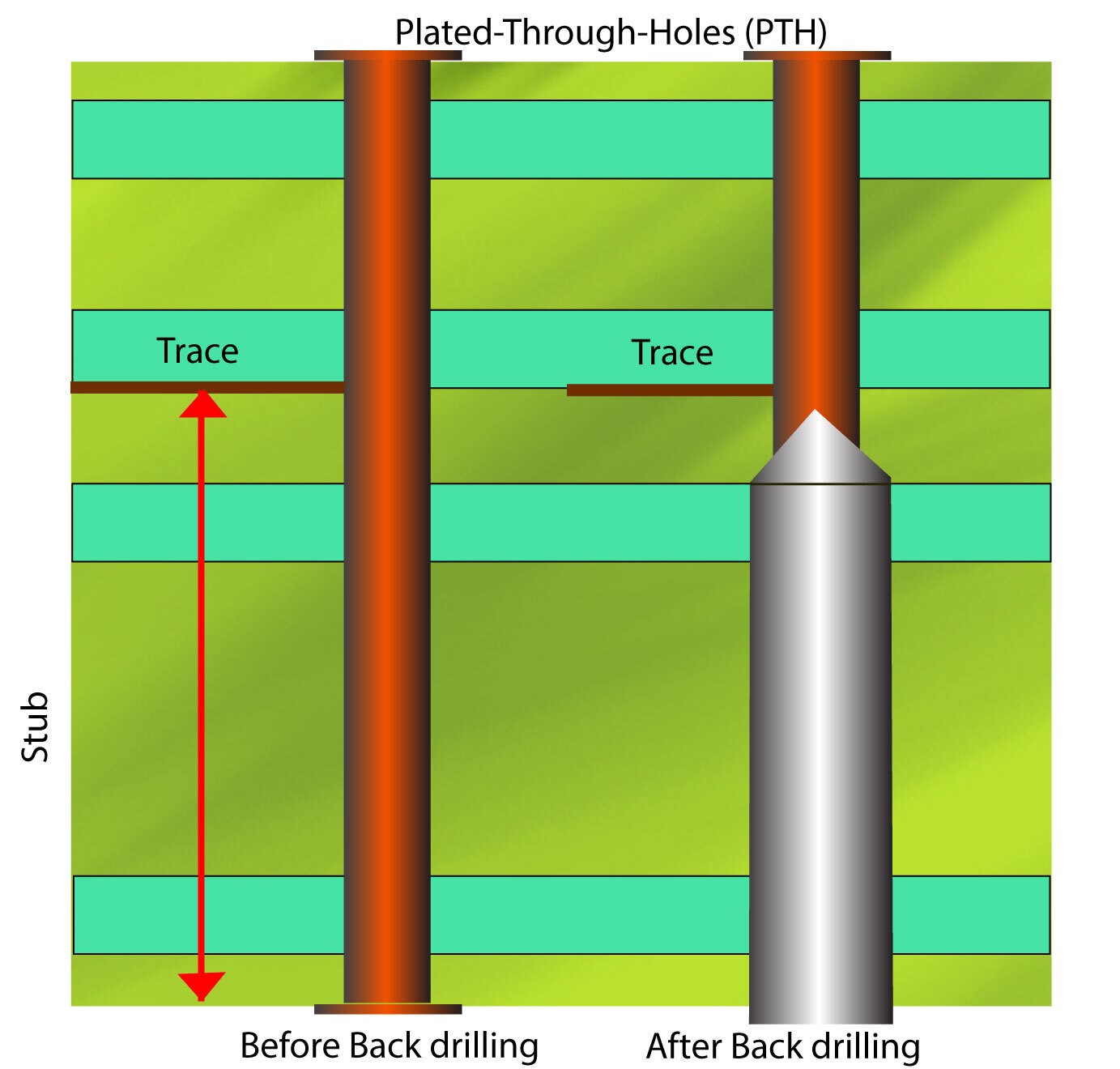
Backdrilling, also known as controlled depth drilling, targets the stub in plated through-hole vias on multilayer PCBs. In a typical setup, a via connects signals across all layers, but if the trace only uses a few layers, the remaining copper barrel acts as a stub. This stub extends beyond the signal path, behaving like an open-ended transmission line that disrupts signals. For electronic hobbyists, understanding PCB backdrilling for beginners starts here: stubs longer than a fraction of the signal wavelength cause unwanted reflections, degrading performance.
Signal reflection reduction becomes crucial as hobby projects scale to gigabit speeds. Common interfaces like Ethernet or DDR memory in custom boards suffer from ringing, overshoot, and eye diagram closure without mitigation. Via stub effects manifest as increased insertion loss and return loss, leading to data errors or system instability. Manufacturers perform backdrilling after via plating by drilling a slightly larger hole from the opposite side, precisely removing the stub while leaving the functional via intact.
The relevance extends to everyday hobbyist designs. Even a simple Arduino shield with high-speed peripherals benefits from cleaner signals. Industry standards like IPC-6012E outline performance specs for rigid boards, emphasizing via integrity for reliable operation. Ignoring stubs might work at low speeds but fails as frequencies rise above a few hundred MHz.
Related Reading: Advanced Backdrilling Design: Optimizing Stackup for High Performance PCBs
Technical Principles Behind Via Stub Effects
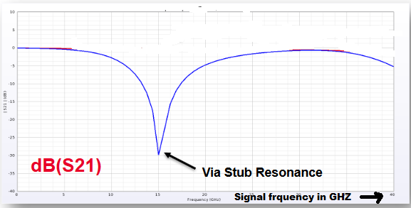
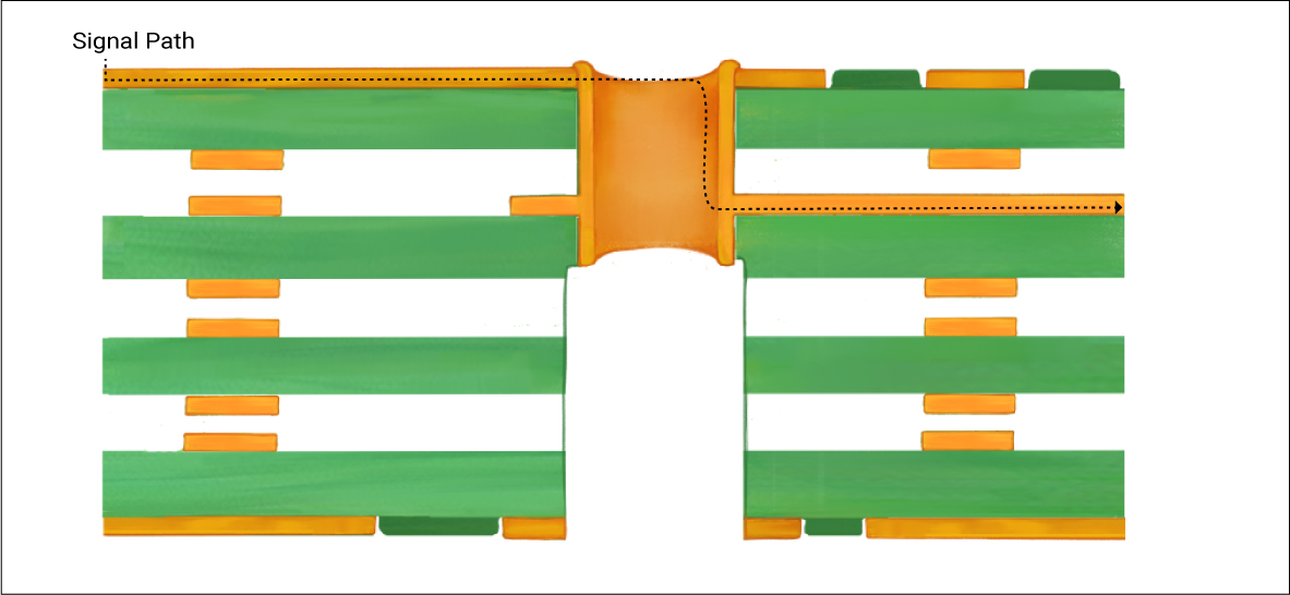
To appreciate backdrilling, consider signals as traveling waves along PCB traces, governed by transmission line theory. Each trace has a characteristic impedance, typically 50 or 100 ohms for single-ended or differential pairs. A via introduces a discontinuity if its stub creates an impedance mismatch. When the signal reaches the stub’s open end, part reflects back, interfering with the incoming wave and causing distortion.
Via stub effects worsen with frequency because the stub’s electrical length grows relative to the wavelength. A rule of thumb for beginners: if the stub exceeds one-tenth of the wavelength, reflections become significant. For a 1 GHz signal in FR-4 material, wavelengths are around 15 cm, so stubs over 1.5 cm cause issues. These reflections add noise, reduce bandwidth, and limit trace lengths in high-speed designs.
Impedance mismatches amplify the problem. The stub acts as a parallel stub resonator, creating resonances that attenuate specific frequencies. In multilayer boards, multiple vias compound these effects, turning a clean eye diagram into a noisy mess. PCB design basics teach that minimizing discontinuities preserves signal quality. Standards such as IPC-2221B provide guidelines on via design to control these mechanisms from the start.
Fabrication tolerances play a role too. Variations in drill depth or plating thickness alter stub lengths, making predictions tricky without simulation. Hobbyists can visualize this through time-domain reflectometry concepts, where reflections appear as voltage steps on a scope.
Basic Backdrilling Techniques for Signal Reflection Reduction
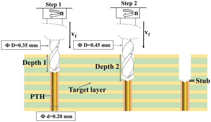
Implementing basic backdrilling techniques starts with planning your layer stackup. Identify nets needing high-speed routing, like clocks or data lines, and mark vias for backdrilling. Specify the backdrill depth to stop just beyond the last signal layer, typically 0.1–0.2 mm clearance. The backdrill diameter is larger than the original via by 5–10 mils to ensure stub removal without hitting the functional barrel.
In design files, note backdrill requirements clearly: pair number, depth from top or bottom, and diameter. Manufacturers use optical or mechanical depth control during the secondary drill after plating. This process leaves a clean shoulder at the transition, verified through cross-section analysis. For PCB backdrilling for beginners, start with symmetric stacks to simplify depths.
Key considerations include spacing. Backdrill holes must avoid adjacent pads or traces to prevent damage. IPC-6012E requires validation holes per panel to confirm depth accuracy, ensuring consistency across production. Hobbyists ordering prototypes should request these coupons for inspection.
Alternatives like blind or buried vias exist but increase cost and complexity. Backdrilling suits through-hole vias economically. Post-process, inspect for roughness or resin smear, which could introduce new losses.
Related Reading: Simulating Backdrilling: How to Optimize PCB Performance Before Manufacturing
Best Practices and Troubleshooting for Hobbyists
Adopt a structured approach to PCB design basics with backdrilling. First, simulate via performance using field solvers to quantify stub impact before committing. Group backdrills by depth to minimize setups, reducing fab costs. Aim for fewer unique depths, say two or three per board.
Troubleshoot via stub effects by measuring return loss with a vector network analyzer if available, or observe eye patterns on a scope. Common issues include incomplete stub removal, showing persistent ringing, or drill wander hitting signals. Verify fab drawings match your specs, and request netlists highlighting backdrill vias.
Layer pairing matters: route high-speed signals on inner layers with ground planes adjacent for better impedance control. Combine backdrilling with length matching and series resistors for robust designs. For electronic hobbyists, test iteratively on prototypes, adjusting based on real-world signals.
Conclusion
PCB backdrilling for beginners unlocks signal reflection reduction by eliminating via stub effects, essential for modern hobby projects. From understanding reflections to applying basic backdrilling techniques, this method enhances reliability without overwhelming complexity. Reference standards like IPC-6012E ensure your designs meet quality benchmarks. Start small, verify results, and scale to faster boards confidently. Your next high-speed prototype will perform smoother, paving the way for advanced electronics.
FAQs
Q1: What is PCB backdrilling for beginners, and when should I use it?
A1: PCB backdrilling removes unused via stubs to improve signal integrity in multilayer boards. Use it for high-speed nets like USB or Ethernet where frequencies exceed 500 MHz, as stubs cause reflections distorting signals. Hobbyists benefit in 4+ layer designs; specify depths clearly in fab notes for reliable results. This technique aligns with PCB design basics without needing exotic vias.
Q2: How do via stub effects impact signal reflection reduction?
A2: Via stubs create impedance discontinuities, reflecting signals back along the trace and causing ringing or loss. Effects intensify at higher frequencies, closing the eye diagram and risking errors. Backdrilling shortens stubs below critical lengths, restoring clean propagation. Monitor with scopes to confirm improvements in hobby prototypes.
Q3: What are basic backdrilling techniques for hobbyist PCBs?
A3: Plan stackups to minimize depths, mark vias in design files, and note larger drill diameters post-plating. Request depth verification coupons per IPC-6012E standards. Space backdrills from pads adequately to avoid damage. This approach suits prototypes, balancing cost and signal reflection reduction effectively.
Q4: Can backdrilling replace other methods for via stub effects?
A4: It complements blind vias or routing adjustments but excels for cost-effective through-hole fixes. Not ideal for ultra-dense boards; combine with ground planes for best results. Hobbyists find it practical for signal reflection reduction in mid-speed designs.
References
IPC-6012E — Qualification and Performance Specification for Rigid Printed Boards. IPC, 2017
IPC-2221B — Generic Standard on Printed Board Design. IPC, 2009
IPC-A-600K — Acceptability of Printed Boards. IPC, 2020