Introduction
Designing a printed circuit board as a hobbyist can be an exciting journey into electronics. However, creating a functional and reliable PCB requires understanding fundamental design rules to ensure manufacturability and performance. For hobbyists, mastering basics like PCB edge considerations and solder mask clearances is critical to avoid common pitfalls. These elements directly impact the structural integrity and soldering quality of your board. This guide, crafted for electronic hobbyists, breaks down essential design principles in a logical and structured manner. Whether you are building a simple LED circuit or a complex microcontroller project, adhering to these guidelines will help you achieve better results. Let's explore the key rules that govern PCB design, focusing on practical tips to elevate your skills and ensure your projects succeed.
What Are PCB Design Rules and Why They Matter
PCB design rules are a set of guidelines that dictate how components, traces, and other elements should be placed and configured on a board. These rules ensure that the PCB can be manufactured without issues and will function as intended. For hobbyists, following design rules is vital to prevent errors like short circuits, poor soldering, or mechanical failures. Ignoring aspects such as PCB edge spacing or solder mask clearances can lead to costly reprints or nonfunctional boards. These rules also align with industry standards, making your designs compatible with professional fabrication processes. Understanding and applying these principles not only improves the quality of your projects but also builds a strong foundation for more advanced PCB work in the future.
Technical Principles of PCB Design Rules
Understanding PCB Edge Considerations
The PCB edge refers to the outer perimeter of the board, and its design plays a significant role in both mechanical stability and manufacturability. Hobbyists must maintain a safe distance between components, traces, and the board's edge to prevent damage during fabrication or handling. A common guideline is to keep all copper traces and components at least 0.5 millimeters away from the edge. This buffer zone protects against accidental cuts or cracks during the milling process. Additionally, if your design includes mounting holes, ensure they are positioned with adequate spacing from the edge to avoid structural weakness. Failing to account for PCB edge spacing can result in broken boards or compromised electrical connections.

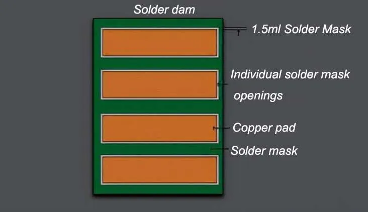
Solder Mask Clearances Explained
Solder mask clearances define the area around copper pads where the solder mask layer is absent, exposing the pad for soldering. This clearance is crucial for ensuring proper solder application during assembly. For hobbyists, a typical solder mask clearance ranges from 0.05 to 0.1 millimeters beyond the pad's edge, depending on the fabrication capabilities. Too small a clearance can lead to solder mask covering part of the pad, causing poor connections. Conversely, excessive clearance might expose adjacent traces, risking short circuits. Following standardized guidelines, such as those in IPC-7351B, helps maintain consistency in pad design and solder mask application. Properly configured clearances improve soldering reliability and reduce defects in your projects.
Related Reading: What is a Solder Mask Bridge in PCB Design?
Trace Width and Spacing Basics
Trace width and spacing are fundamental to ensuring electrical performance and safety. Wider traces can carry more current, while adequate spacing prevents crosstalk or shorting between adjacent lines. For hobbyist projects with low current needs, a trace width of 0.25 millimeters is often sufficient. Spacing between traces should be at least equal to the trace width to minimize interference. In high voltage designs, larger spacing is necessary to prevent arcing, often guided by standards like IPC-2221B. Hobbyists should always check their design against the current carrying capacity and voltage requirements to avoid overheating or failure.
Related Reading: Understanding Trace Width Tolerances in PCB Manufacturing for Reliable Designs
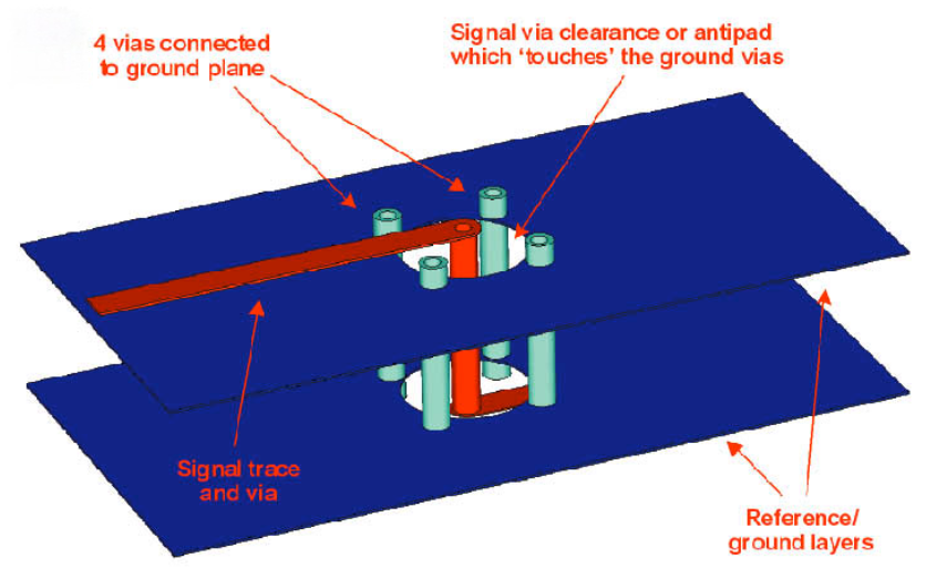
Via and Drill Hole Guidelines
Vias connect different layers of a PCB, and their design must adhere to specific rules for reliability. The drill hole size for vias should be chosen based on the current they will carry and the manufacturing constraints. A common minimum drill size for hobbyist boards is 0.3 millimeters, with an annular ring of at least 0.15 millimeters around it for stability. Ensure that vias are placed away from the PCB edge to avoid mechanical stress. Adhering to guidelines from standards like IPC-6012E ensures that vias are manufacturable and robust enough for your application.
Practical Solutions and Best Practices for Hobbyists
Planning PCB Edge Layouts
When designing your board, always start by defining the PCB edge and outlining keep out zones. Use your design software to set a restricted area of at least 0.5 millimeters from the edge where no components or traces are allowed. If your project requires a specific board shape, ensure that cutouts or slots are clearly marked and avoid sharp internal corners that could stress the material. For boards that will be panelized, consider adding breakaway tabs with mouse bites for easy separation after fabrication. These steps help protect the integrity of your board during production and use.
Setting Up Solder Mask Clearances
To achieve optimal solder mask clearances, consult the fabrication guidelines provided by your manufacturer, as capabilities can vary. As a general rule, aim for a clearance of 0.075 millimeters around each pad to balance exposure and protection. In your design software, adjust the solder mask layer to ensure it does not overlap with pads or vias intended for soldering. Double check the design before submission to confirm that all exposed areas are intentional. Following standards like IPC-SM-840E can guide you in selecting appropriate solder mask parameters for durability and performance.
Component Placement Tips
Place components logically, grouping related parts together to minimize trace lengths. Keep sensitive components away from the PCB edge to avoid mechanical damage. Ensure that taller components do not obstruct access to mounting holes or connectors. For surface mount devices, align pads with consistent solder mask clearances to facilitate assembly. Always leave enough space between components for heat dissipation and ease of soldering, especially in manual assembly typical for hobbyists. Reviewing placement against IPC-7351B guidelines can help standardize your approach.
Design Review and Validation
Before finalizing your design, perform a thorough review using design rule checks in your software. Verify that PCB edge spacing, solder mask clearances, and trace widths meet the required specifications. Check for unconnected nets or overlapping elements that could cause issues. If possible, generate a 3D view of your board to visualize component heights and edge clearances. Following a systematic validation process reduces the likelihood of errors and ensures your design aligns with manufacturing expectations as outlined in IPC-A-600K.
Troubleshooting Common Hobbyist Mistakes
Hobbyists often encounter issues due to overlooking basic design rules. A frequent error is placing components too close to the PCB edge, leading to damage during handling or fabrication. To fix this, always enforce a keep out zone in your layout. Another common mistake is incorrect solder mask clearances, resulting in soldering defects. Review your solder mask layer to ensure proper pad exposure, adjusting clearances as needed. Additionally, insufficient trace spacing can cause shorts, especially in dense designs. Use design rule checks to identify and correct spacing violations before production. Learning from these mistakes helps hobbyists refine their skills and produce more reliable boards over time.
Conclusion
Mastering basic PCB design rules is essential for hobbyists aiming to create functional and durable boards. Focusing on elements like PCB edge spacing and solder mask clearances ensures manufacturability and performance. By understanding the technical principles behind trace widths, via placement, and component layouts, you can avoid common errors and improve your projects. Implementing practical solutions, such as design validation and adherence to industry standards, builds confidence in your work. As you grow as a designer, these foundational guidelines will serve as a stepping stone to tackling more complex challenges in electronics design.
FAQs
Q1: What is the minimum PCB edge spacing for hobbyist designs?
A1: For hobbyist PCB designs, a minimum edge spacing of 0.5 millimeters is recommended between the board's edge and any traces or components. This buffer prevents damage during fabrication and handling. Always check your design software to enforce a keep out zone and ensure structural integrity, especially if your board includes custom shapes or mounting holes.
Q2: Why are solder mask clearances important in PCB design?
A2: Solder mask clearances are critical because they define the exposed area of copper pads for soldering. Proper clearance, typically 0.05 to 0.1 millimeters, ensures reliable solder joints without covering pads or exposing adjacent traces. Incorrect clearances can lead to soldering defects or shorts, impacting the functionality of your hobbyist project.
Q3: How do I avoid mistakes with PCB edge placement?
A3: To avoid PCB edge placement errors, set a restricted area in your design software at least 0.5 millimeters from the edge. Keep components and traces within this zone to prevent mechanical damage. Review your layout using design rule checks and consider the board's shape or panelization needs before finalizing the design.
Q4: What standards should hobbyists follow for solder mask clearances?
A4: Hobbyists should refer to industry standards like IPC-SM-840E for solder mask application and IPC-7351B for pad design guidelines. These standards provide specifications for clearances and material properties, ensuring consistency and reliability. Following them helps align your design with manufacturing capabilities, reducing the risk of assembly issues.
References
IPC-7351B - Generic Requirements for Surface Mount Design and Land Pattern Standard. IPC, 2010.
IPC-2221B - Generic Standard on Printed Board Design. IPC, 2012.
IPC-6012E - Qualification and Performance Specification for Rigid Printed Boards. IPC, 2020.
IPC-A-600K - Acceptability of Printed Boards. IPC, 2020.
IPC-SM-840E - Qualification and Performance of Permanent Solder Mask and Flexible Cover Materials. IPC, 2010.


