Introduction
Ball Grid Array (BGA) packages have become a cornerstone in modern PCB design due to their ability to support high pin counts in compact footprints. These packages are widely used in applications requiring dense interconnects, such as microprocessors and memory chips. Routing with BGA packages presents unique challenges, including managing vias, microvias, and routing channels while leveraging High-Density Interconnect (HDI) techniques. For electrical engineers, understanding these elements is vital to ensure signal integrity and manufacturability. This article explores the essentials of routing BGA packages, focusing on practical strategies and industry standards. By mastering these concepts, designers can optimize layouts for performance and reliability in complex electronic systems.
What Are BGA Packages and Why Do They Matter
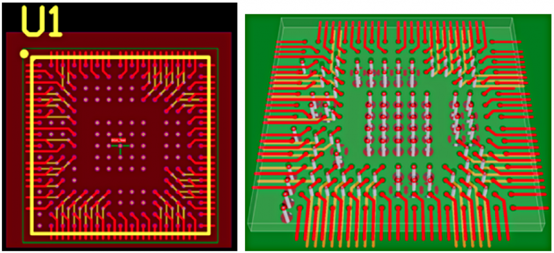
BGA packages are surface-mount components with an array of solder balls on the underside for connection to a PCB. Unlike traditional packages with peripheral leads, BGAs distribute connections across the entire bottom surface, allowing for higher pin density. This makes them ideal for devices requiring numerous connections in limited space. Their importance lies in enabling miniaturization and improved thermal performance in modern electronics. However, routing these packages demands precision due to tight spacing and complex signal requirements. Effective BGA routing ensures minimal crosstalk, controlled impedance, and reliable assembly, directly impacting device functionality. For engineers, mastering BGA layout techniques is essential to meet the demands of high-speed and high-density designs.
Technical Principles of Routing BGA Packages
Routing BGA packages involves understanding several key elements, including vias, microvias, and the structure of routing channels. Each plays a critical role in connecting the dense array of BGA pads to other layers or components on the PCB.
Vias and Microvias in BGA Routing
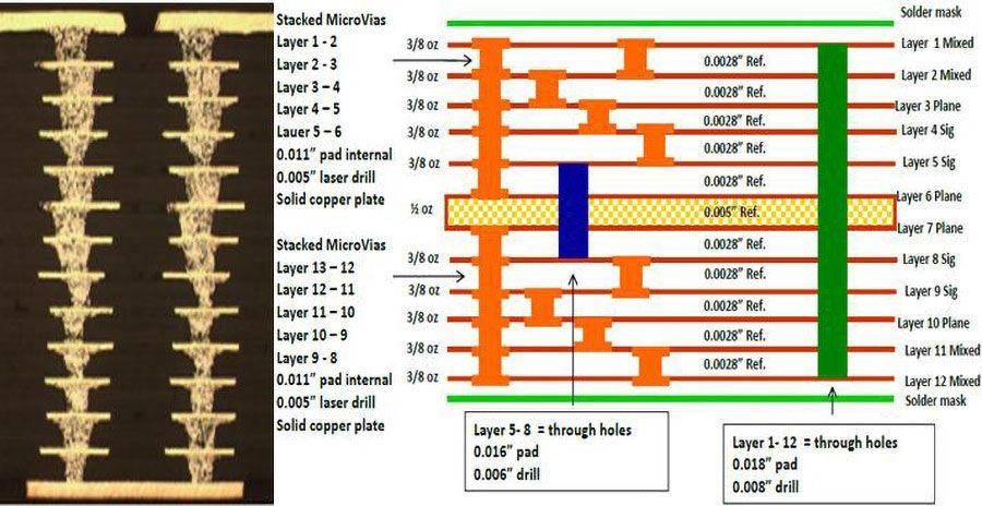
Vias are conductive pathways that connect different layers of a PCB. In BGA designs, standard vias often cannot fit within the tight pitch of the solder balls, necessitating smaller solutions. Microvias, which are significantly smaller in diameter, are commonly used in HDI designs to address this issue. These tiny vias allow connections directly from BGA pads to inner layers without consuming excessive space. According to industry standards such as IPC-2226, microvias must meet specific aspect ratio and reliability criteria to ensure performance during thermal cycling and assembly processes.
Routing Channels and Escape Patterns
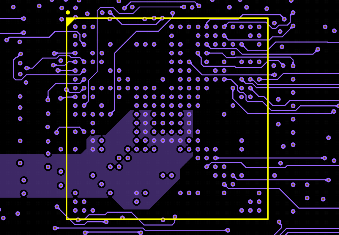
Routing channels refer to the pathways between BGA pads where traces are placed to escape the dense grid of connections. For fine-pitch BGAs, often below 0.5 mm, escape routing becomes challenging. Engineers typically use a combination of microvias and strategic trace placement to fan out signals to outer layers. A common approach is the dog-bone pattern, where a short trace connects the BGA pad to a microvia, allowing signals to transition to another layer. Proper planning of these channels prevents signal congestion and maintains clearance as defined by standards like IPC-6012E.
High-Density Interconnect Techniques
HDI technology is integral to BGA routing, enabling the use of microvias and finer traces in multilayer boards. This approach supports higher wiring density, crucial for compact designs. HDI layouts often incorporate stacked or staggered microvias to optimize space and improve signal routing. Adhering to guidelines in IPC-2226 for HDI design ensures that these structures maintain reliability under mechanical and thermal stress. This methodology is particularly effective for managing the complex interconnects required by modern BGA packages.
Practical Solutions for Routing BGA Packages
Achieving successful routing with BGA packages requires actionable strategies tailored to the constraints of high-density designs. Below are best practices that electrical engineers can implement to optimize their layouts.
Optimize Via Placement and Type
Place microvias directly in or near BGA pads, often using via-in-pad technology, to minimize trace length and inductance. Ensure that non-conductive fill is used for via-in-pad designs to prevent solder wicking during assembly, as recommended by IPC-7095D. This standard provides detailed guidance on BGA assembly and via design to avoid defects. Balance the use of through-hole vias for power and ground connections with microvias for signals to manage board space effectively.
Plan Escape Routing Early
Develop a clear escape routing strategy before starting the layout. For fine-pitch BGA packages, prioritize inner rows for critical signals and use outer rows for less sensitive connections. Allocate routing channels systematically to avoid bottlenecks. Use multilayer boards with dedicated ground and power planes to simplify signal escape and reduce interference. Following design rules from IPC-2221B ensures proper spacing and clearance during this process.
Leverage HDI for Complex Designs
Incorporate HDI techniques for BGAs with pitches below 0.65 mm. Use stacked microvias to connect multiple layers without increasing board size. Ensure that trace widths and spacing comply with HDI-specific standards like IPC-2226 to maintain signal integrity. This approach allows more routing channels in constrained areas, supporting the dense interconnects typical of BGA layouts.
Manage Signal Integrity
Maintain controlled impedance for high-speed signals by routing traces with consistent widths and avoiding sharp bends. Place ground planes adjacent to signal layers to provide a return path and reduce noise. Use simulation tools to verify signal performance before fabrication, aligning with best practices outlined in IPC-2141A for high-speed design. Proper via placement also minimizes stub effects that can degrade signal quality.
Consider Thermal and Mechanical Constraints
Account for thermal expansion and mechanical stress during routing. Avoid placing vias or traces in areas prone to stress, such as near board edges or under large components. Ensure that BGA pad designs follow IPC-7095D for optimal solder joint reliability. This standard addresses thermal management and pad geometry to prevent issues like cracking or delamination during operation.
Troubleshooting Common BGA Routing Challenges
Engineers often encounter specific issues when routing BGA packages. Addressing these challenges requires a systematic approach grounded in industry standards.
Congested Routing Channels
When routing channels are too narrow, signals may interfere or fail to escape the BGA grid. Resolve this by increasing layer count or using HDI techniques with microvias. Adjust trace widths to the minimum allowed by IPC-6012E to create additional space. Prioritize critical nets and route them first to secure optimal paths.
Signal Crosstalk and Noise
Crosstalk arises from closely spaced traces in dense BGA layouts. Mitigate this by maintaining adequate spacing as per IPC-2221B and routing high-speed signals on separate layers. Use ground vias strategically to shield sensitive traces. Verify designs against signal integrity guidelines in IPC-2141A to ensure minimal interference.
Assembly Defects from Poor Via Design
Improper via placement or type can lead to solder joint failures during assembly. Avoid using large through-hole vias under BGA pads, as they can cause voids. Instead, opt for microvias with non-conductive fill, following IPC-7095D recommendations. This prevents solder wicking and ensures reliable connections.
Conclusion
Routing with BGA packages is a complex but essential skill for modern PCB design. By understanding the roles of vias, microvias, and routing channels, engineers can create efficient layouts for high-density applications. Leveraging HDI techniques further enhances design capabilities, allowing for finer pitches and compact boards. Adhering to industry standards ensures reliability and manufacturability, addressing challenges like signal integrity and thermal stress. With careful planning and strategic implementation, successful BGA routing becomes achievable, paving the way for innovative and robust electronic systems.
FAQs
Q1: What are the main challenges in routing BGA packages?
A1: Routing BGA packages is challenging due to tight pin spacing and high density. Fine pitches, often below 0.5 mm, limit routing channels and increase crosstalk risks. Managing vias and microvias for escape routing while maintaining signal integrity adds complexity. Following standards like IPC-7095D helps mitigate assembly issues and ensures reliable connections in these compact layouts.
Q2: How do microvias improve BGA routing efficiency?
A2: Microvias enhance BGA routing by enabling connections in tight spaces where standard vias cannot fit. Their small diameter supports HDI designs, allowing direct links from BGA pads to inner layers. This reduces trace length and inductance, improving signal performance. As per IPC-2226, microvias must meet specific reliability criteria to withstand thermal and mechanical stress.
Q3: Why is HDI technology critical for BGA packages?
A3: HDI technology is vital for BGA packages because it supports finer traces and stacked microvias in multilayer boards. This allows higher wiring density, crucial for fine-pitch BGAs. It optimizes space and simplifies complex routing, ensuring signal integrity. Guidelines in IPC-2226 ensure HDI structures maintain performance in demanding applications with dense interconnects.
Q4: How can routing channels be optimized for BGA layouts?
A4: Optimizing routing channels for BGA layouts involves early planning of escape patterns and prioritizing critical signals. Use microvias for inner rows and allocate outer rows for less sensitive nets. Increase layer count if needed and follow IPC-6012E for spacing rules. This approach prevents congestion and ensures efficient signal escape in dense designs.
References
IPC-2221B — Generic Standard on Printed Board Design. IPC, 2012.
IPC-2226 — Sectional Design Standard for High Density Interconnect (HDI) Printed Boards. IPC, 2003.
IPC-6012E — Qualification and Performance Specification for Rigid Printed Boards. IPC, 2020.
IPC-7095D — Design and Assembly Process Implementation for Ball Grid Arrays (BGAs). IPC, 2018.
IPC-2141A — Design Guide for High-Speed Controlled Impedance Circuit Boards. IPC, 2004.


