Why Are Blind Vias Essential in Modern PCB Layouts?
For PCB designers aiming to maximize space, boost signal integrity, and control costs in intricate multilayer board designs, mastering the use of blind vias is fundamental. These specialized vias connect internal layers of a printed circuit board without extending through the entire substrate, making them particularly advantageous for high-density interconnect (HDI) designs. This guide will delve into crucial blind via PCB design rules, strategies for manufacturability, a step-by-step tutorial for Altium users, and essential best practices to help you produce efficient and dependable PCB layouts.
Whether you are new to PCB design or an experienced professional, this comprehensive overview provides actionable insights, practical examples, and technical details to refine your design capabilities. Let’s explore the world of blind vias and learn how to implement them effectively in your upcoming projects.
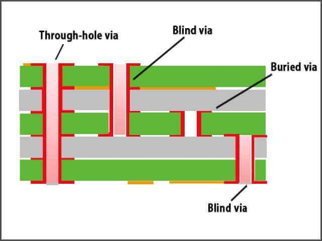
What Exactly Are Blind Vias, and Why Do They Matter?
Blind vias are a distinct type of via in PCB design, engineered to connect two or more inner layers of a multilayer board without reaching either outer surface. Unlike traditional through-hole vias, which traverse the entire board thickness, blind vias are drilled and plated only to a specified depth, appearing "invisible" from one side of the PCB.
The significance of blind vias stems from their capacity to conserve board space and enhance design efficiency. By enabling vias to be stacked vertically (along the z-axis), they free up valuable surface area that can then be used for additional components and traces. Moreover, they significantly improve signal integrity by shortening trace lengths, which in turn reduces inductance and minimizes signal loss. For instance, in high-speed applications, these shorter connections can reduce signal propagation delay by as much as 20-30% compared to typical through-hole vias in specific configurations.
From a cost perspective, blind vias can also eliminate the necessity for more complex through-hole plating processes, potentially leading to a 10-15% reduction in manufacturing expenses for HDI PCB designs. However, to fully realize these benefits, designers must strictly adhere to specific design guidelines and manufacturing constraints. We will now examine these in greater detail.
What Are the Key Design Rules for Blind Vias?
Designing PCBs with blind vias demands meticulous attention to specific rules to ensure both functionality and manufacturability. Here are the critical blind via PCB design rules that every designer should implement:
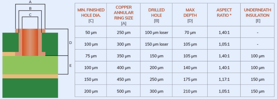
● Aspect Ratio Constraints: The aspect ratio, defined as the depth-to-diameter ratio of a blind via, is crucial for achieving reliable plating and drilling. Most manufacturers advise an aspect ratio of 1:1 or less for blind vias. For example, a via with a 0.2 mm diameter should not exceed a 0.2 mm depth to prevent potential plating defects.
● Minimum Drill Size: Blind vias typically require smaller drill sizes compared to their through-hole counterparts. A standard minimum drill size for blind vias is around 0.15 mm (6 mils), though this can vary based on the specific capabilities of the manufacturer.
● Precise Layer Stack-Up Planning: Blind vias must be carefully planned in accordance with the PCB's layer stack-up. They are intended to connect only the specified internal layers without encroaching upon or interfering with other layers. For a 6-layer board, a blind via might link layers 1 to 2 or 2 to 3, but not extend further.
● Clearance and Spacing: Adequate spacing is essential between blind vias and other board features, such as traces and pads. A common guideline is to maintain a minimum clearance of 0.2 mm (8 mils) to prevent short circuits or manufacturing defects.
● Signal Integrity Considerations: In high-speed designs operating at frequencies above 1 GHz, blind vias play a vital role in reducing stub effects, which can degrade signal quality. Position them strategically to minimize impedance mismatches, ideally maintaining a characteristic impedance of 50 ohms for most RF applications.
Strict adherence to these rules ensures that your PCB design is not only functionally sound but also readily manufacturable. Neglecting them can lead to issues such as incomplete plating, drilling inaccuracies, or compromised signal performance.
How to Design Blind Vias for Optimal Manufacturability?
Designing blind vias with manufacturability as a priority is crucial to avoid costly revisions and production delays. Here are essential tips for ensuring your blind via designs are production-ready:
● Consult Manufacturer Guidelines Early: Fabrication houses have diverse capabilities regarding blind via drilling and plating. Some may support microvias down to 0.1 mm (4 mils), while others might be limited to 0.2 mm (8 mils). Always verify these specifications with your chosen manufacturer before finalizing your design.
● Limit Via Stacking Complexity: While stacking blind vias can be effective for space-saving, excessive stacking (more than two sequential vias) significantly complicates manufacturing and can increase costs by up to 25%. Employ stacked vias only when absolutely necessary for critical areas.
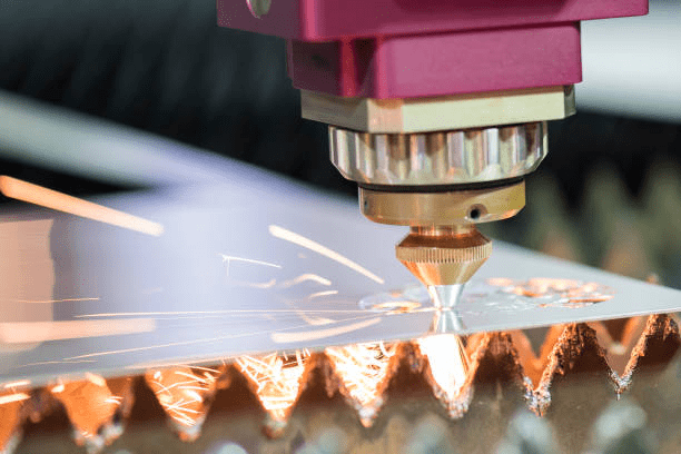
● Optimize Via Depth Control: Blind vias demand highly precise depth control during the drilling process. Laser drilling is often utilized for microvias to achieve accuracies typically within ±0.025 mm. Ensure your design specifies via depths that align with these tight tolerances.
● Avoid Overlapping Vias: Overlapping blind vias on different layer pairs can create structural weaknesses within the PCB. Maintain a minimum offset of 0.3 mm (12 mils) between vias on adjacent layer pairs to preserve board integrity.
● Strategic Material Selection: Choose PCB materials that are compatible with blind via manufacturing processes. For instance, high-Tg (glass transition temperature above 170°C) FR-4 materials are frequently preferred for HDI PCBs due to their ability to withstand the thermal stresses associated with microvia laser drilling.
By prioritizing these manufacturability aspects, you can significantly reduce the likelihood of production errors and ensure a smoother transition from design concept to final fabrication.
Step-by-Step Altium Blind Via Tutorial
For designers utilizing popular PCB design software like Altium Designer, configuring blind vias can be straightforward with the correct procedure. This Altium blind via tutorial will guide you through the process of creating and setting up blind vias within your projects.
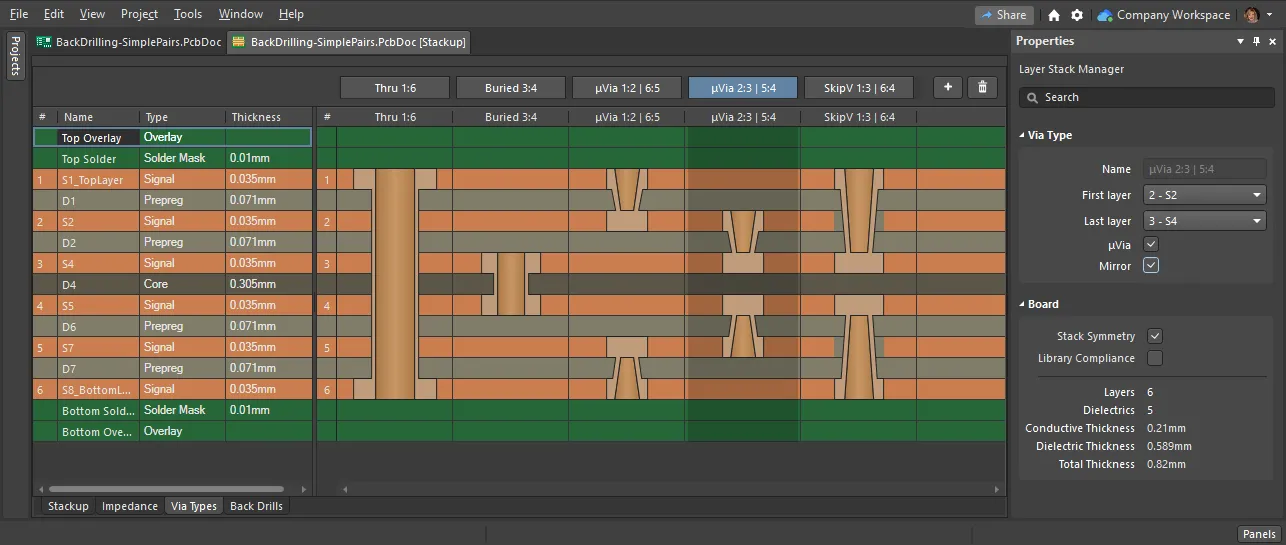
1. Define the Layer Stack: Begin by accessing the Layer Stack Manager in your design software. Carefully define the number of layers and their intended connections. For a 6-layer board, for example, you might configure blind vias to connect layers 1-2 and 5-6.
2. Set Via Types: In the via properties panel, select "Blind" as the designated via type. You will then specify the precise start and stop layers for each individual blind via. For instance, a via intended to connect layers 1 to 2 should have a start layer of 1 and a stop layer of 2.
3. Adjust Via Dimensions: Configure the via diameter and drill size according to your established design rules. A common setting for blind vias involves a diameter of 0.3 mm (12 mils) with a corresponding drill size of 0.2 mm (8 mils).
4. Place the Via: Utilize the dedicated via placement tool to accurately position the blind via within your PCB layout. Ensure that its placement aligns correctly with the nets connecting the specified layers. The software will automatically restrict the via to operate within its defined layer range.
5. Verify Design Rules: Execute a comprehensive Design Rule Check (DRC) to confirm that the blind via adheres to all clearance, spacing, and manufacturability constraints. Make any necessary adjustments to resolve detected violations.
6. Generate Manufacturing Outputs: When preparing and exporting Gerber files or drill data, ensure that the blind via specifications are clearly articulated. Include a detailed fabrication note explicitly stating the via type and the exact layer connections to eliminate ambiguity.
Following these precise steps ensures that blind vias are correctly implemented within your design tool, thereby minimizing potential errors during the fabrication process. Always perform a thorough double-check of the output files to confirm that all blind via data is accurately represented.
What Are the Best Practices for Maximizing Blind Via Performance?
To achieve optimal results with blind vias, adhering to specific best practices is crucial for enhancing performance, ensuring reliability, and simplifying manufacturing.
● Strategic Use in High-Density Areas: Reserve blind vias for regions of your board where space is at a premium, such as beneath BGA (Ball Grid Array) components with very tight pitches, sometimes as fine as 0.5 mm. This allows for highly efficient routing without sacrificing valuable board real estate.
● Balance Cost with Complexity: While blind vias can potentially reduce costs by eliminating the need for full through-hole plating, they can conversely increase expenses if they are overused or improperly designed. Aim for a sensible balance, employing them only where absolutely necessary, typically in designs featuring 6 or more layers.
● Simulate Signal Performance: For high-speed applications, always use simulation tools to thoroughly analyze the impact of blind vias on signal integrity. Ensure that key metrics like return loss remain below -15 dB and insertion loss is minimized, particularly for frequencies exceeding 5 GHz.
● Collaborate with Fabricators: Early and continuous collaboration with your fabrication partner is a crucial step in preventing potential design issues. Share your detailed layer stack-up and via specifications to confirm they align perfectly with the manufacturer’s capabilities, thereby significantly reducing the risk of production delays.
● Thorough Prototype Testing: After the fabrication process, rigorously test your prototype board for electrical continuity and signal performance. Employ specialized tools such as a Time-Domain Reflectometer (TDR) to verify that blind vias maintain precise impedance control, ideally within ±10% of the target value (e.g., 50 ohms).
Implementing these best practices will enable you to create robust PCB designs that consistently meet both demanding performance benchmarks and stringent manufacturing requirements.
What Are Common Blind Via Challenges and Their Solutions?
While blind vias offer numerous advantages, designers must also anticipate and address certain inherent challenges. Here are some common issues and their effective solutions:
● Drilling Accuracy Issues: Inaccurate drilling depth can result in incomplete or unreliable connections.
○ Solution: Utilize laser drilling for microvias and specify tight tolerances (e.g., ±0.025 mm) within your design files and manufacturing instructions.
● Plating Deficiencies: Poor plating within blind vias can lead to open circuits, compromising board functionality.
○ Solution: Maintain a low aspect ratio (1:1 or less) and partner with manufacturers who employ advanced plating techniques, such as reverse pulse plating, to ensure uniform copper deposition.
● Cost Overruns: Overly complex blind via designs can significantly inflate PCB manufacturing costs.
○ Solution: Strategically limit the number of blind via sequences and optimize their placement to minimize manufacturing complexity and associated expenses.
● Signal Stub Effects: Unused portions of vias can act as signal stubs, which can degrade signal quality, particularly in high-speed applications.
○ Solution: Design blind vias to terminate precisely at the required layer, actively avoiding any unnecessary extensions that could create these detrimental stubs.
By proactively anticipating these challenges and applying the suggested solutions, you can effectively mitigate risks and ensure a successful outcome for your blind via designs.
Conclusion: Elevate Your PCB Designs Through Blind Vias
Blind vias represent a formidable tool for PCB designers, offering significant benefits in space optimization, enhanced signal integrity, and cost efficiencies within multilayer and HDI designs. By diligently adhering to established blind via PCB design rules, emphasizing design for manufacturability, leveraging software tools as demonstrated in our Altium blind via tutorial, and implementing crucial best practices, you can create high-performing, reliable circuit boards that meet the rigorous demands of modern electronics.
Confidently integrate blind vias into your next project. Utilize the comprehensive guidelines and practical tips provided in this guide to skillfully navigate the complexities of both design and manufacturing, thereby ensuring that your PCBs are not only innovative but also eminently practical. With meticulous planning and precise execution, blind vias have the potential to revolutionize your approach to PCB layout, unlocking new possibilities for creating compact, high-speed, and advanced designs.


