Introduction
Through-hole components remain essential in PCB design for applications requiring mechanical strength and high power handling. These components, inserted through drilled holes and soldered on the opposite side, provide robust connections that withstand vibration and thermal stress better than surface-mount alternatives in certain scenarios. Proper footprint design ensures secure mounting, preventing issues like loose fits, solder joint failures, or component misalignment during assembly. Engineers must consider lead dimensions, hole tolerances, and pad geometries to achieve reliable performance. This article explores footprint creation principles for through-hole components, focusing on axial components, radial components, and DIP packages. By adhering to established guidelines, designers can optimize hole size calculation and overall PCB design for long-term durability.
Footprint design directly impacts manufacturability and assembly yield. Inaccurate dimensions lead to challenges in automated insertion or wave soldering processes. Secure mounting translates to reduced rework and enhanced product reliability in demanding environments. Understanding these fundamentals equips electrical engineers to create footprints that balance space efficiency with mechanical integrity.
What Are Through-Hole Components and Why Does Footprint Design Matter?
Through-hole components feature leads that pass through plated holes in the PCB, forming mechanical and electrical bonds via solder fillets. Common examples include axial components like resistors and capacitors with straight leads bent for insertion, radial components such as electrolytic capacitors with parallel leads extending from the body, and DIP packages used for integrated circuits with dual rows of pins. These differ from surface-mount types by relying on hole interference and solder for retention. Footprint design defines the precise layout of holes, pads, and silkscreen markings to match component geometry.
Footprint design matters because it ensures secure mounting under operational stresses. Poorly designed footprints result in lead-hole mismatches, causing components to shift during soldering or vibrate loose over time. In high-reliability applications, such as aerospace or automotive electronics, this can lead to failures. Industry standards like IPC-7251 provide guidelines for land patterns, emphasizing density levels that dictate hole and pad sizes. Accurate PCB design minimizes these risks while supporting efficient assembly flows.
The relevance extends to mixed-technology boards where through-hole components coexist with SMT parts. Designers must account for thermal expansion differences to avoid stress concentrations. Secure footprints also facilitate rework and inspection, aligning with quality control protocols. Ultimately, thoughtful footprint creation enhances the entire PCB lifecycle from prototyping to production.
Technical Principles of Footprint Design for Through-Hole Components
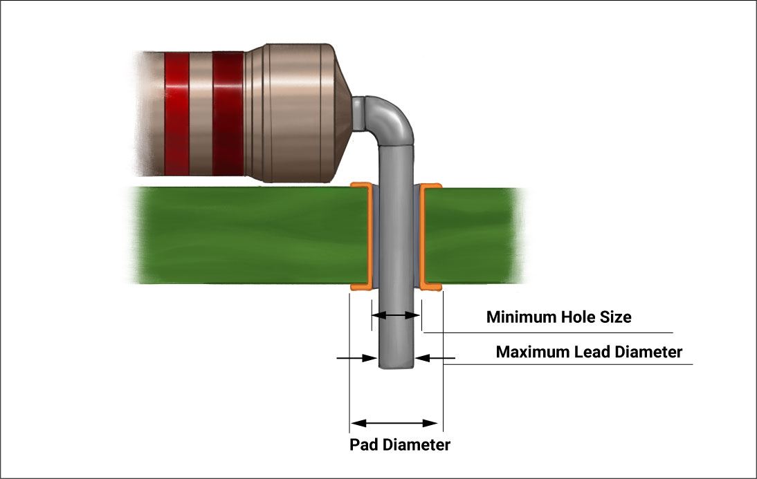
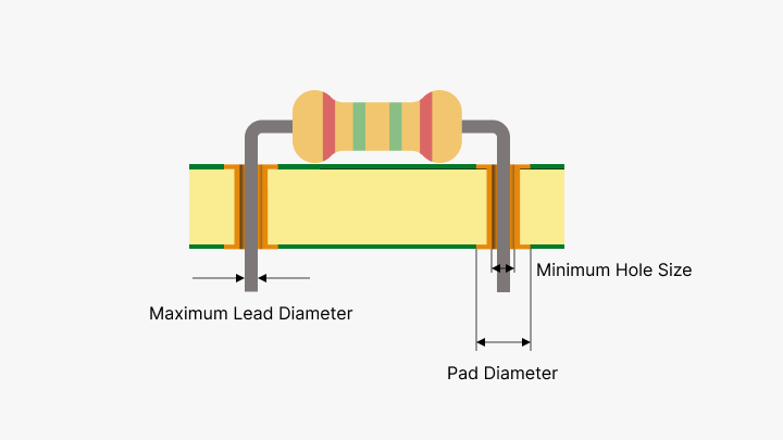
Footprint design begins with analyzing component datasheets for lead diameter, length, body size, and pitch. Holes must accommodate leads with sufficient clearance for insertion while allowing solder wicking for strong joints. Pad annuli provide electrical connection and mechanical support, typically sized larger than the finished hole diameter. Silkscreen outlines and polarity markers aid assembly precision. These elements collectively ensure secure mounting by distributing forces evenly.
Hole size calculation follows standardized approaches based on maximum lead diameter and plating thickness. The finished hole size includes drill diameter minus plating buildup, with clearance determined by assembly density. IPC-2221B outlines generic rules for board design, including thru-hole vias and component holes, stressing minimum annular ring widths for etch tolerance. Engineers select conservative sizes to prevent breakout or weak barrels. This principle underpins reliable plating and soldering.
Pad design complements holes by extending beyond the annulus for fillet formation. The pad-to-hole ratio influences solder joint strength, with larger pads offering better heat dissipation during wave soldering. Component spacing prevents interference, especially for high-pin-count parts like DIP packages. Courtyard boundaries define keep-out zones for automated placement. These technical aspects form the foundation of robust footprint design.
Thermal and mechanical considerations further refine footprints. Coefficient of thermal expansion mismatches between component leads and PCB material can induce stress, so generous clearances mitigate cracking. Vibration-prone designs benefit from dual-sided soldering where feasible. Fabrication tolerances, such as drill wander, necessitate oversizing holes slightly. Integrating these principles yields footprints optimized for secure mounting across lifecycles.
Footprint Design Specifics for Axial, Radial, and DIP Components
Axial Components
Axial components, prevalent in resistors and film capacitors, have leads extending from opposite body ends. Footprint design orients holes parallel to the board edge, spaced according to body length plus lead form allowances. Leads bend into a U-shape for vertical mounting, requiring holes positioned to align with formed leads. Secure mounting relies on tight lead-hole fits to resist torque during insertion.
Hole size calculation for axial parts prioritizes maximum lead diameter plus clearance for plating. Pads flank each hole symmetrically, sized to support solder ramps on both sides. Silkscreen indicates bend direction and standoff height to prevent board shorts. Variations in lead plating thickness demand verification against datasheet tolerances. This structured approach ensures axial components mount securely without excessive play.
Radial Components
Radial components feature leads emerging parallel from one body side, ideal for polarized capacitors. Footprints place holes side-by-side, spaced by lead pitch with vertical offset for body clearance. Mounting orients the body perpendicular to the board, leveraging gravity for insertion stability. Hole size calculation mirrors axial but accounts for lead stagger in some packages.
Pads extend outward to form broad fillets, enhancing joint strength against radial pull forces. Polarity arcs on silkscreen prevent reverse insertion errors. For high-capacitance electrolytics, footprints include vent slots nearby for safety. Secure mounting demands precise pitch to avoid lead stress fractures. Engineers adjust for manufacturing tolerances to maintain reliability.
DIP Packages
DIP packages house ICs with two parallel rows of pins, used in legacy and prototyping designs. Footprint design aligns holes in staggered rows matching pin pitch, typically 2.54 mm or 15.24 mm row spacing. Secure mounting requires uniform hole sizing across all pins to ensure flat seating. Extended pads accommodate pin trimming variations.
Hole size calculation balances insertion ease with solder retention, per density guidelines. Index holes or notches aid orientation during automated handling. Courtyards prevent adjacent component crowding. For socketed DIPs, footprints incorporate anti-rotation features. This precision ensures stable mounting under thermal cycling.
Best Practices for Ensuring Secure Mounting
Adopt IPC-7251 density levels: A for most relaxed, B/C for high-density with tighter clearances. Verify footprints against 3D models for interference checks. Simulate solder joint profiles using fillet height criteria from J-STD-001 to predict strength. Incorporate fiducials near high-precision areas for alignment.
Panelize footprints with test coupons for plating thickness validation. Use symmetric pad shapes to minimize warpage during reflow if mixed assembly. Document tolerances explicitly in fabrication notes. These practices yield secure mounting with high assembly yields.
Collaborate early with fabricators on drill capabilities. Prototype small runs to inspect hole quality post-plating. Iterate based on cross-section analysis for annulus integrity. Consistent application prevents field failures.
Common Challenges and Troubleshooting
Misaligned holes from drill tolerances cause insertion jams; mitigate with oversized clearances. Excessive clearance leads to solder wicking shorting; tighten per density level. Bent leads in axial parts stress joints; specify form radii in datasheets.
Thermal mismatch cracks barrels; select low-Tg materials or add relief slots. Verify footprints in viewer tools pre-gerber export. Troubleshooting involves root-cause analysis via X-ray or sectioning.
Conclusion
Mastering footprint creation for through-hole components secures mounting and elevates PCB design reliability. From hole size calculation to pad optimization, attention to axial, radial, and DIP specifics pays dividends in performance. Standards like IPC-7251 and J-STD-001 guide these efforts logically. Engineers applying structured principles achieve robust assemblies ready for demanding applications. Prioritize verification at every stage for optimal outcomes.
FAQs
Q1: How do you calculate hole size for through-hole components in PCB design?
A1: Hole size calculation starts with the maximum lead diameter from the datasheet, adding clearance based on IPC-7251 density levels, such as Level B or C for production boards. Account for plating thickness, typically 25 microns, to determine finished hole size. This ensures easy insertion while supporting strong solder joints. Always verify against fabrication capabilities to avoid undersizing.
Q2: What are key differences in footprint design for axial versus radial components?
A2: Axial components use longitudinally spaced holes matching body length, with leads bent for vertical stance. Radial footprints position holes transversely with parallel leads for upright body mounting. Both require pad extensions for fillets, but radials emphasize pitch accuracy for polarization. Secure mounting demands tailored clearances per component type.
Q3: Why is pad sizing critical for DIP packages in through-hole PCB design?
A3: Pad sizing for DIP packages provides annular ring support and solder fillet area, preventing pin float during wave soldering. Oversized pads dissipate heat evenly across rows, reducing voids. Proper ratios per standards ensure mechanical retention under vibration. This directly impacts footprint design reliability.
Q4: What best practices ensure secure mounting of through-hole components?
A4: Follow J-STD-001 for termination requirements, selecting density-appropriate hole-pad combos. Include silkscreen for orientation and 3D checks for clashes. Prototype to confirm plating uniformity. These steps minimize assembly defects and enhance longevity.
References
IPC-7251 — Generic Requirements for Through-Hole Design and Land Pattern Standard. IPC.
IPC-2221B — Generic Standard on Printed Board Design. IPC.
J-STD-001H — Requirements for Soldered Electrical and Electronic Assemblies. IPC, 2018.


