Introduction
Component footprints form the foundation of successful surface mount technology (SMT) assembly, directly influencing how pick-and-place machines position parts on the board. These land patterns, consisting of solder pads, solder mask openings, and reference features, must accommodate precise component placement while ensuring robust solder joints through reflow soldering. Poorly designed footprints can lead to misalignment, insufficient solder volume, or defects like bridging and tombstoning, which disrupt high-volume production lines. Engineers optimizing for pick-and-place machines focus on tolerances that allow self-alignment during reflow, reducing the demand for sub-micron placement accuracy. This article explores footprint design principles, integration with solder paste stencils, and assembly guidelines to enhance SMT assembly efficiency and reliability. By following established practices, designers can minimize troubleshooting and maximize throughput in automated processes.
Understanding Component Footprints in SMT Assembly
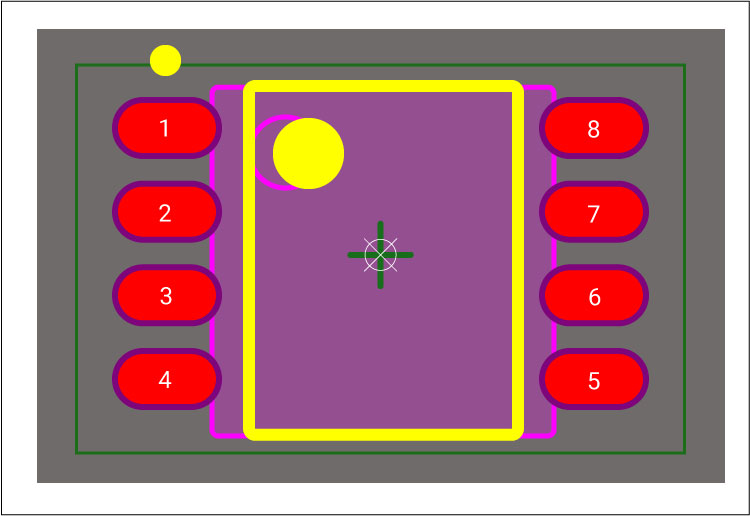
A component footprint represents the physical layout of pads and associated features on a PCB where surface mount devices (SMDs) are placed and soldered. In SMT assembly, pick-and-place machines rely on the footprint's origin point, typically the geometric center or pin 1 indicator, to accurately position components onto solder paste deposits. This origin serves as the reference for machine coordinates exported from design files, ensuring components align with pads despite minor offsets. Footprints must balance pad size for solder wetting against spacing to prevent shorts, especially in high-density boards. Why does this matter for pick-and-place? Optimized footprints enable higher placement speeds by providing margin for machine tolerances, typically around 50-100 microns, while promoting capillary action that centers components during reflow. Troubleshooting starts here: mismatched footprints from datasheets lead to chronic placement errors visible in post-reflow inspection.
Key Principles of Component Footprint Design
Footprint design begins with component dimensions from manufacturer datasheets, including lead pitch, body size, and tolerance stacks. Pads are shaped to promote uniform solder flow, such as rectangular for QFPs or oval for chip resistors to reduce tombstoning risks. The IPC-7351B standard outlines three density levels: Level A (least dense, largest pads for rework), Level B (nominal for general use), and Level C (most dense, smallest pads for compact layouts). Selecting the right level depends on assembly capabilities; nominal often suits high-speed pick-and-place by offering placement tolerance without excessive solder volume. Courtyards around footprints define keep-out zones, preventing adjacent parts from interfering with machine nozzles or vision systems. Always incorporate polarity marks, like a half-moon pad or bar code, for orientation verification during automated handling.
Optimizing Footprints for Pick-and-Place Machines
Pick-and-place machines use vision systems to recognize component outlines and leads, then place them onto paste-covered footprints with high precision. Footprint optimization involves standardizing the origin at the component center, aligning with industry conventions to avoid rotation offsets in assembly files. Symmetric pad layouts enhance self-centering via surface tension in reflow, forgiving slight misplacements common in high-throughput lines. For fine-pitch parts like BGAs, toe and heel fillet dimensions per IPC guidelines ensure joints form reliably even if placement shifts by 25% of pad width. Panel fiducials aid board alignment, but footprint consistency across the design reduces programming time for feeders and heads. In practice, test prototypes reveal if footprints allow nozzle clearance, preventing collisions during placement cycles.
Integration with Solder Paste Stencils and Reflow Soldering
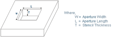
Solder paste stencils translate footprint geometry into precise apertures for paste deposition, critical before pick-and-place. The IPC-7525C standard guides stencil thickness and aperture shapes, recommending reductions for fine-pitch to control volume and avoid bridging. Apertures typically match pad outlines but may include home plating or trapezoidal forms to improve paste release. After placement, reflow soldering melts the paste, forming fillets that meet J-STD-001J criteria for joint integrity. Footprints with balanced pad areas prevent hot spots or voids, ensuring even heating profiles. Troubleshooting stencil-footprint mismatches often uncovers insufficient paste, leading to opens; always validate volumes through SPI (solder paste inspection) in the assembly line.
Best Practices and Assembly Guidelines
Follow datasheet footprints first, then adjust per density needs using validated libraries to avoid custom errors. Export centroid files with accurate X-Y coordinates and theta rotations for pick-and-place programming. Maintain minimum courtyard spacing of 0.25 mm between footprints to accommodate machine vision fields. For mixed-technology boards, segregate SMT zones to optimize feeder setups. Simulate reflow with thermal models to predict joint formation from footprint paste volumes. Panelize boards with breakaway tabs and fiducials spaced for machine tables, typically every 100 mm. These assembly guidelines streamline SMT processes, cutting cycle times and defect rates.
In high-volume runs, standardize on nominal density for versatility across suppliers. Verify footprints with 3D models or DFM checks before Gerber release. Orient all passives consistently, like 0 degrees, to simplify tape-and-reel feeding.
Common Challenges and Troubleshooting in Footprint Optimization
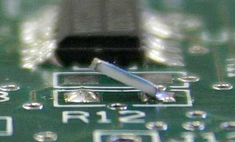
Misaligned placements often stem from origin shifts between design tools and assembly software; cross-verify centroids early. Tombstoning in chip components signals uneven pad areas or excessive paste on one end, fixable by symmetrizing footprints. Solder bridging arises from oversized pads or poor stencil release, addressed by density Level C reductions. Insufficient wetting appears as dewet or voids, tracing to undersized pads; upscale per IPC-7351B while checking reflow profiles. Post-placement offsets show in X-ray, prompting fiducial recalibration or footprint tweaks for better self-alignment. Systematic DFM reviews catch these before production, saving costly respins.
Conclusion
Optimizing component footprints bridges design intent with SMT assembly realities, enabling pick-and-place machines to deliver high yields through precise placement and reliable reflow. Adhering to standards like IPC-7351B for land patterns, IPC-7525C for stencils, and J-STD-001J for joints ensures robust processes. Practical guidelines—standard origins, balanced pads, and courtyard margins—minimize defects while supporting speed. Engineers troubleshooting assemblies find most issues root in footprint geometry, underscoring early validation. Implementing these strategies elevates PCB reliability and production efficiency in demanding applications.
FAQs
Q1: What role does IPC-7351B play in component footprint design for SMT assembly?
A1: IPC-7351B provides standardized land pattern geometries across density levels A, B, and C, tailored to assembly needs. It defines pad dimensions, shapes, and tolerances to optimize solder joints and placement tolerance for pick-and-place machines. Using these reduces defects like bridging or opens, ensuring compatibility with reflow soldering. Designers select levels based on board density and rework priorities for reliable outcomes.
Q2: How do footprints affect pick-and-place accuracy in SMT assembly?
A2: Footprints define the placement target via origin points and pad layouts, allowing self-centering during reflow to tolerate minor offsets. Symmetric designs and clear polarity marks aid machine vision recognition. Proper courtyards prevent nozzle interference, supporting high-speed operations. Mismatches cause chronic misalignment, resolved by centroid file verification and standard orientations.
Q3: What are key assembly guidelines for solder paste stencils with SMT footprints?
A3: Align stencil apertures closely to footprint pads per IPC-7525C, using shapes that promote clean release. Balance paste volume to avoid excess leading to bridges or deficits causing voids. Validate through print tests before pick-and-place. Thickness selection matches component pitch for uniform deposition in reflow soldering.
Q4: How can engineers troubleshoot reflow soldering issues tied to footprint design?
A4: Inspect joints against J-STD-001J criteria; uneven fillets indicate pad imbalance. X-ray reveals voids from poor paste volume. Adjust density levels or stencil reductions accordingly. Thermal profiling confirms even heating. Prototype runs identify self-alignment limits for pick-and-place tolerances.
References
IPC-7351B — Generic Requirements for Surface Mount Design and Land Pattern Standard. IPC, 2010
IPC-7525C — Stencil Design Guidelines. IPC, 2021
J-STD-001J — Requirements for Soldered Electrical and Electronic Assemblies. IPC, 2024


