Introduction
High-speed PCBs operate at frequencies where signal wavelengths approach the physical dimensions of traces and components, leading to challenges like electromagnetic interference (EMI) and signal loss. Proper component placement becomes critical to maintain signal integrity, minimize crosstalk, and ensure reliable performance in applications such as telecommunications, computing, and data centers. Engineers must prioritize layout strategies that reduce inductive and capacitive coupling while preserving controlled impedance. This article explores high-speed PCB component placement techniques focused on EMI reduction and signal loss mitigation. Key elements include strategic positioning of high-frequency components, decoupling capacitors, termination resistors, and ground planes. By following these structured approaches, designers can achieve robust designs compliant with industry expectations for performance and reliability.
Why Component Placement Matters in High-Speed PCBs
In high-speed environments, signals propagate as transmission lines rather than lumped elements, making trace lengths and component positions influential factors in overall system behavior. Poor placement can induce EMI through radiated emissions from large current loops or conducted noise via power rails. Signal loss occurs due to reflections from impedance discontinuities, dielectric absorption, and conductor losses, all exacerbated by suboptimal layouts. Effective high-speed PCB component placement shortens critical paths, minimizes via counts, and optimizes return currents, directly impacting bit error rates and eye diagram quality. Ground planes serve as low-impedance return paths, but their effectiveness depends on component proximity to these planes. Understanding these interactions allows engineers to predict and mitigate issues early in the design cycle.
EMI reduction requires isolating sensitive analog sections from digital noise sources, while signal loss demands matched impedances across the board. Components like clocks and transceivers generate the most interference if not carefully placed. Layout strategy influences thermal management too, as clustered high-frequency components may require dedicated heat sinking. Compliance with standards such as IPC-2221 reinforces these principles by outlining spacing and placement guidelines for electrical performance.
Fundamental Principles Behind EMI and Signal Loss
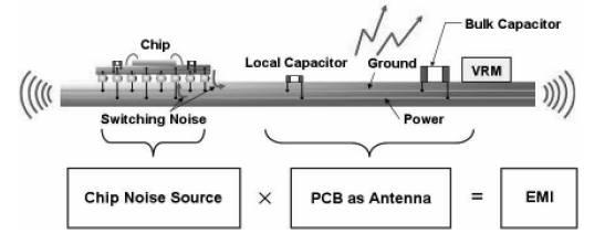
Electromagnetic interference arises from time-varying electric and magnetic fields coupling into unintended paths, with common-mode currents on I/O lines amplifying radiation. In high-speed PCBs, trace inductance forms loops that act as antennas, especially when return paths are distant. Signal loss manifests as attenuation, where skin effect confines currents to conductor surfaces, increasing resistance at gigahertz frequencies. Impedance mismatches cause reflections, quantified by return loss in decibels, degrading high-speed data transmission. Decoupling capacitors provide local charge reservoirs to suppress voltage droops from switching transients. A continuous ground plane under signal layers confines fields, reducing both EMI and crosstalk by providing a predictable return path.
Return path integrity is paramount; discontinuities like splits in ground planes force currents to detour, elevating inductance and EMI. High-frequency components demand short, wide traces to lower series resistance and reactance. Termination resistors absorb reflections by matching characteristic impedance, typically 50 or 100 ohms for differential pairs. These principles guide layout strategy, ensuring fields remain confined between signal and reference planes. Engineers simulate these effects using field solvers to validate placements before fabrication.
Best Practices for High-Speed PCB Component Placement
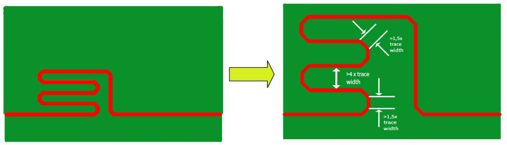
Start with high-frequency components by grouping them near connectors or interfaces to shorten critical nets and reduce stub lengths. Place transceivers and clock drivers centrally or adjacent to their primary loads, minimizing fanout traces that could radiate EMI. This high-speed PCB component placement strategy also facilitates length matching for skew-sensitive signals like DDR memory buses. Avoid placing unrelated low-speed parts in these zones to prevent noise pickup. Surrounding these areas with guard traces tied to ground further aids EMI reduction.
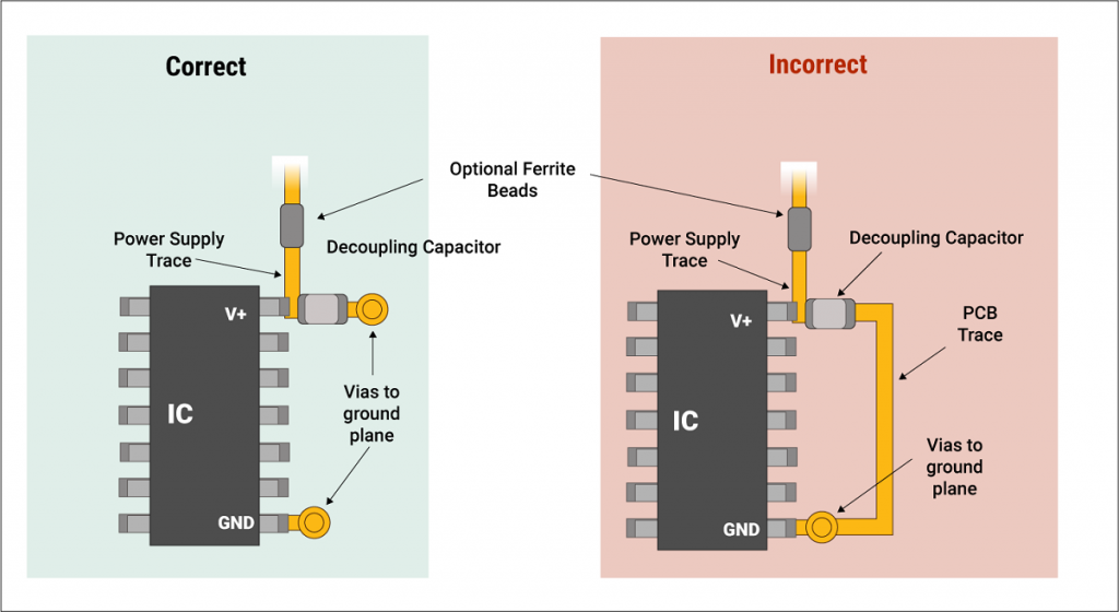
Decoupling capacitors must sit as close as possible to IC power pins, ideally within 1-2 mm, with vias directly connecting to power and ground planes. Multiple values, such as 0.1 μF and 10 μF ceramics, in parallel provide broadband decoupling, shunting noise across frequencies. Position them under the IC if using via-in-pad technology, ensuring low-inductance paths. This placement combats signal loss from power supply ripple coupling into outputs. Ground vias around the capacitor enhance current spreading, aligning with IPC-2141A guidelines for controlled impedance in high-speed designs.
Termination resistors belong at the receiver end for source-series setups or midway for some backplanes, precisely tuned to line impedance. Place them adjacent to the terminated pin to avoid stubs that reflect high-frequency content. Surface-mount 0402 or 0603 packages minimize parasitics, and dedicate nearby ground vias for heat dissipation. Integrating them into the signal path reduces board space while preserving signal integrity. Monitor for thermal hotspots, as power dissipation scales with frequency.
A solid ground plane on inner layers, unbroken except for necessary splits, anchors all return currents and shields against external EMI. Pour copper generously around component pads, stitching edges with vias every few millimeters to equalize potentials. For multi-layer boards, dedicate layers alternately as signal-ground pairs to confine fields. This layout strategy significantly cuts signal loss by stabilizing impedance.
Route high-speed signals orthogonally to adjacent layers to suppress broadside coupling, and pair differential lines tightly with equal lengths. Keep power distribution symmetric, with decoupling at every rail transition. Simulate post-layout to verify eye openings exceed margins. Common pitfalls include via farms under BGA balls disrupting planes or clocks routed over splits. Iterative refinement ensures EMI reduction without sacrificing density.
Advanced Layout Strategies and Troubleshooting
For densely packed boards, employ floorplanning tools to pre-place high-frequency components, reserving zones for analog and digital domains separated by ground corridors. Active devices like PLLs benefit from isolated ground islands returned at a single point to prevent noise loops. In troubleshooting EMI, probe suspect nets with near-field scanners to identify radiating loops, then adjust placements iteratively. Signal loss diagnostics involve TDR measurements revealing impedance bumps from poor via transitions.
Hybrid designs mixing RF and baseband require shielded enclosures around high-frequency components, with feedthrough capacitors for DC blocks. Monitor stackup symmetry to avoid warpage impacting connector mating. These strategies, rooted in engineering fundamentals, yield predictable performance.
Conclusion
Strategic high-speed PCB component placement directly addresses EMI reduction and signal loss through minimized loop areas, optimal decoupling, precise termination, and robust ground planes. Engineers achieve this by prioritizing critical nets, simulating rigorously, and adhering to proven layout strategies. These practices not only enhance signal integrity but also streamline manufacturing and testing. Implementing them early prevents costly respins, ensuring designs meet demanding speed requirements reliably.
FAQs
Q1: What is the ideal placement for decoupling capacitors in high-speed PCB component placement?
A1: Decoupling capacitors should be positioned within millimeters of IC power and ground pins, with direct vias to planes for low inductance. Use multiple capacitor values for frequency coverage, placing them under the package if feasible. This layout strategy suppresses noise, aiding EMI reduction and preventing signal loss from supply droops. Ground stitching around vias distributes currents effectively.
Q2: How does a ground plane contribute to EMI reduction in high-speed PCBs?
A2: A continuous ground plane provides a low-impedance return path, confining magnetic fields and reducing radiation from current loops. Place it adjacent to signal layers to maintain impedance control and minimize crosstalk. Avoid splits under high-speed traces, stitching any gaps densely. This foundational element is key in any high-speed PCB component placement plan.
Q3: Where should termination resistors be placed for optimal signal integrity?
A3: Termination resistors go at the receiver end or source as per topology, close to the signal pin to eliminate stubs. Match their value to characteristic impedance precisely. Nearby ground vias handle dissipation and returns. Proper placement cuts reflections, preserving eye quality in high-frequency components.
Q4: What layout strategy minimizes signal loss in high-speed designs?
A4: Group high-frequency components near interfaces, use short matched traces, and ensure unbroken reference planes. Orthogonal routing between layers reduces coupling. Decoupling and termination support this by stabilizing supplies and ends. Simulations validate the strategy before commit.
References
IPC-2221A — Generic Standard on Printed Board Design. IPC.
IPC-2141A — Design Guide for High-Speed Controlled Impedance. IPC.


