Introduction
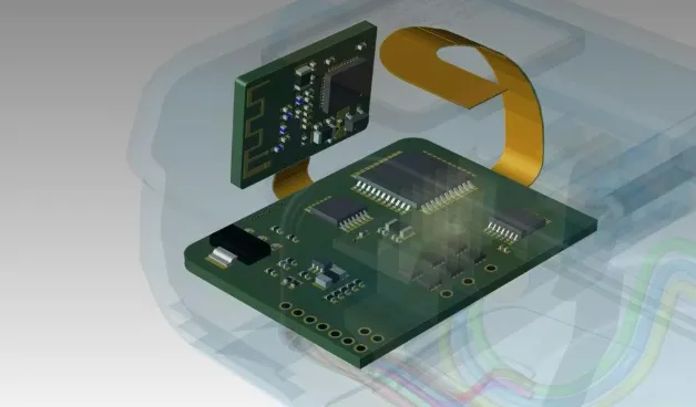
Flexible and rigid-flex printed circuit boards represent critical advancements in electronics packaging, allowing designs to fit into tight spaces while maintaining electrical performance. Engineers face unique challenges in managing constraints such as mechanical flexibility, signal integrity, and material compatibility during the design phase. Effective constraint management ensures long-term reliability in applications ranging from wearables to aerospace systems. This article explores key techniques for handling flexible PCB design constraints, rigid-flex PCB layout issues, bend radius constraints for flex PCBs, material selection for flex PCBs, and impedance control for flex PCBs. By applying structured approaches, designers can optimize these boards for production and use. Adhering to established guidelines minimizes risks like cracking, delamination, or signal degradation.

Why Constraint Management Matters in Flex and Rigid-Flex PCBs
Constraint management directly impacts the mechanical durability and electrical functionality of flexible and rigid-flex PCBs. In dynamic environments, improper bend radius constraints for flex PCBs can lead to conductor fatigue over time. Similarly, poor material selection for flex PCBs may cause thermal mismatches during assembly or operation. Rigid-flex PCB layout demands careful zoning to separate rigid component areas from flexible interconnects, preventing stress concentrations. Impedance control for flex PCBs becomes complex due to varying dielectric thicknesses in bend regions. Ultimately, mastering these constraints aligns designs with performance classes defined in IPC-6013, enhancing yield and lifespan.
Without disciplined constraint handling, prototypes often fail qualification tests, delaying projects and increasing costs. Engineers must balance form factor demands with manufacturability from the outset. This proactive strategy supports higher assembly success rates and field reliability.
Core Technical Principles of Flexible PCB Design Constraints
Flexible PCB design constraints stem from the inherent properties of thin substrates and ductile conductors. Copper traces in flex circuits experience tensile and compressive stresses during bending, necessitating wider traces and rounded corners to distribute forces evenly. Layer count influences flexibility, with single-layer designs tolerating tighter radii than multilayers. Substrate materials must exhibit low modulus for repeated flexing while providing adequate insulation. Electrical constraints arise from thinner dielectrics, affecting capacitance and crosstalk in high-density routing. IPC-2223 outlines these principles, specifying parameters for circuit types like static or dynamic applications.
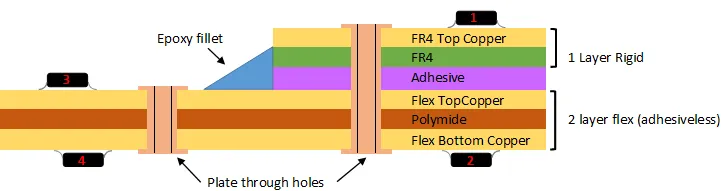
In rigid-flex configurations, constraints extend to transition zones where rigid and flexible sections join. Adhesives and coverlays must bond securely without introducing voids that compromise integrity. Thermal expansion differences between rigid epoxy and flex polyimide require staggered vias and relief features. Signal paths crossing bends demand consistent trace geometry to preserve characteristic impedance. These mechanisms highlight the need for simulation tools during early layout stages.
Bend Radius Constraints for Flex PCBs: Engineering Fundamentals
Bend radius constraints for flex PCBs define the minimum curvature allowable without damaging conductors or substrates. The radius scales with copper thickness and layer count, as thicker constructions resist deformation less effectively. For static bends, where flexing occurs infrequently, guidelines permit tighter radii compared to dynamic scenarios involving millions of cycles. Engineers calculate effective radius by considering the neutral axis shift within the stackup. Exceeding limits induces micro-cracks in copper plating, leading to open circuits. IPC-2223 provides tabulated values based on bend type and construction, guiding conservative designs.
Routing orientation plays a pivotal role, with traces perpendicular to the bend axis experiencing maximum strain. Annular rings around vias in bend areas must incorporate teardrops to avoid tearing. Coverlay openings require precise alignment to prevent exposure. Testing protocols simulate lifecycle stresses, validating radius choices empirically. By prioritizing these factors, designs achieve robustness across temperature ranges.
Material Selection for Flex PCBs: Balancing Flexibility and Performance
Material selection for flex PCBs involves evaluating dielectric properties, thermal stability, and mechanical endurance. Polyimide films dominate due to their high glass transition temperature and low moisture absorption, ideal for harsh environments. Adhesive choices, such as acrylic or epoxy-based, affect peel strength and flex life. Conductor foils, rolled annealed copper preferred over electrodeposited for ductility, influence bend performance. Constraints include matching coefficients of thermal expansion with rigid sections in hybrid boards. Dimensional stability under humidity demands materials with controlled shrinkage.
Coverlay and bondply thicknesses impact overall stackup flexibility and impedance. Thinner layers enhance bendability but reduce voltage standoff. Engineers assess trade-offs using datasheets focused on elongation at break and modulus. Qualification per IPC-6013 verifies material suitability through flex endurance and thermal shock tests. Selecting compatible combinations prevents issues like adhesive flow during lamination.
Impedance Control Techniques for Flex PCBs
Impedance control for flex PCBs requires precise stackup control amid varying geometries. Microstrip and stripline configurations adapt differently to bends, with ground planes providing return paths in rigid sections. Dielectric constant fluctuations in flex regions necessitate wider traces or adjusted spacings. Thicker cores in controlled impedance designs trade flexibility for tolerance. Transition zones demand length-matched routing to minimize reflections. Field solvers predict values, accounting for coverlay effects.
In rigid-flex layouts, impedance continuity across sections relies on consistent reference planes. Vias introduce discontinuities, mitigated by back-drilling or stubs. Manufacturing tolerances for flex etching tighten to ±10% for high-speed signals. Verification involves time-domain reflectometry post-fabrication. These techniques ensure signal integrity in compact assemblies.
Suggested Reading: The Impact of Impedance Control on Signal Integrity in High Speed Rigid Flex PCB Assembly
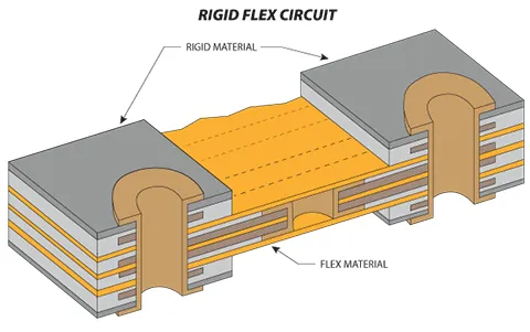
Rigid-Flex PCB Layout: Navigating Hybrid Constraints
Rigid-flex PCB layout constraints center on defining rigid, flex, and transition zones clearly. Component placement confines to rigid areas, avoiding flex tails under mechanical stress. Interconnect traces fan out gradually in transitions to reduce density. Bend axes align perpendicular to vias, spaced at least 10 times the flex thickness apart. Stiffeners reinforce connector sites without impeding flex motion. Layer alignment during lamination demands precise registration holes.
Routing in flex sections favors straight lines parallel to bends, minimizing jogs. Power and ground planes segment to accommodate folding. Solder mask and silkscreen omit from dynamic bends to prevent cracking. Design rules checkers enforce clearances, preventing overlaps. This structured layout supports automated assembly while preserving flexibility.
Best Practices for Implementing Constraint Management
Start with schematic capture incorporating flex-specific symbols for tails and stiffeners. Stackup planning iterates early, modeling bend radii and impedances iteratively. Use zoning layers in layout software to visualize constraints visually. Prototype with scoring for rigid-flex separation, validating form factor. Collaborate with fabrication partners for DFM reviews targeting bend areas.
Document bend cycles and environments in specs, driving material choices. Simulate thermal-mechanical stresses using finite element analysis. Post-layout audits confirm compliance with IPC guidelines. Incremental testing, from static bends to thermal cycling, builds confidence. These practices streamline from concept to production.
Conclusion
Constraint management techniques empower engineers to harness the full potential of flexible and rigid-flex PCBs. Addressing bend radius constraints for flex PCBs, material selection for flex PCBs, impedance control for flex PCBs, and rigid-flex PCB layout systematically ensures reliable outcomes. Logical application of principles from IPC-2223 and IPC-6013 minimizes risks and optimizes performance. Designers achieve compact, durable solutions by integrating these strategies throughout the process. Future designs will leverage advancing materials and tools for even tighter constraints.
FAQs
Q1: What are the primary flexible PCB design constraints engineers must address?
A1: Flexible PCB design constraints include mechanical limits like bend radius, material ductility, and electrical factors such as impedance variation. Engineers prioritize trace width in bend zones to prevent fatigue and select low-modulus substrates for dynamic use. Layout rules enforce perpendicular routing to axes, reducing strain. Compliance with IPC-2223 ensures these constraints align with application demands, supporting high yields. (62 words)
Q2: How do you determine bend radius constraints for flex PCBs in practice?
A2: Bend radius constraints for flex PCBs depend on layer count, copper thickness, and static versus dynamic flexing. Guidelines from IPC-2223 tabulate minimums, such as multiples of total thickness. Engineers factor in cycle life, using simulations for validation. Conservative choices, like 10 times thickness for multilayers, enhance durability. Testing confirms performance under expected conditions. (68 words)
Q3: Why is material selection critical for flex PCBs under thermal stress?
A3: Material selection for flex PCBs focuses on polyimide's thermal stability and CTE matching with rigid parts. Constraints arise from adhesive flow and delamination risks during soldering. High Tg materials resist warpage, while thin films preserve flexibility. IPC-6013 qualification tests verify endurance. Balanced choices prevent failures in reflow processes. (54 words)
Q4: What techniques ensure impedance control for flex PCBs in high-speed designs?
A4: Impedance control for flex PCBs involves stackup optimization with consistent dielectric spacing and reference planes. Flex regions require adjusted trace geometries to compensate for coverlay effects. Rigid-flex transitions use matched lengths to avoid mismatches. Tolerance specs tighten manufacturing, verified by TDR. This maintains signal integrity across bends. (58 words)
References
IPC-2223E — Sectional Design Standard for Flexible Printed Boards and Rigid-Flex Printed Boards. IPC.
IPC-6013E — Qualification and Performance Specification for Flexible Printed Boards. IPC, 2021.
IPC-6012E — Qualification and Performance Specification for Rigid Printed Boards. IPC.