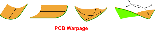
What Causes Warpage in Large PCB Panels?
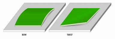
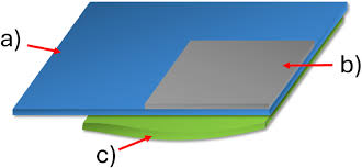
Warpage, or the unwanted bending and deformation of a Printed Circuit Board (PCB) panel, poses a significant challenge in electronics manufacturing, particularly for larger boards. This deviation from a perfectly flat surface can critically compromise the subsequent assembly of components, the integrity of solder joints, and the overall reliability and performance of the electronic device. For engineers, maintaining panel flatness is paramount for producing high-quality, dependable products.
Warpage primarily arises from various stresses—thermal, mechanical, and material-related—introduced during the manufacturing process. Large PCB panels, often utilized to enhance production efficiency, are especially susceptible to these deformations due to their size and the intricate interactions between different materials and processing steps. Industry standards, such as IPC-6012, define acceptable warpage limits, typically ranging from 0.05% for highly reliable Class 4 applications to 0.2% for general-purpose Class 1 boards, measured as a percentage of the board's length.
Primary Factors Contributing to PCB Warpage
Several key elements contribute to the phenomenon of warpage in substantial PCB panels:
● Thermal Stressors: Manufacturing processes like soldering or reflow involve intense heating and cooling cycles. Uneven thermal distribution during these stages can create significant temperature gradients, which in turn induce stresses that cause bending. For instance, a mere 100°C temperature difference across a panel can lead to noticeable deformation, particularly in boards exceeding 300 mm.
● Material Property Mismatches: Different materials within a PCB, such as copper (with a Coefficient of Thermal Expansion, CTE, of 17 ppm/°C) and FR-4 substrate (14-18 ppm/°C), expand and contract at different rates when heated or cooled. This CTE mismatch results in differential expansion, a major driver of warpage.
● Imbalanced Copper Distribution: An uneven distribution of copper across different layers of a PCB creates asymmetrical internal stresses. A panel where one side has, for example, 70% copper coverage while the other has only 30% is highly prone to twisting and bending.
● Panel Design and Processing Weaknesses: Large panels often incorporate V-cut dividers or are subjected to specific handling in reflow furnaces. These elements can compromise the panel's structural integrity or lead to uneven weight distribution, thereby increasing the risk of warpage.
● Thin Substrates: The industry's trend toward thinner PCBs (e.g., 0.8 mm or less) exacerbates warpage issues, as reduced substrate thickness inherently lowers mechanical stability and rigidity.
Consequences of PCB Warpage on Performance
Warpage can severely impact a PCB's functional integrity and long-term reliability. A perfectly flat PCB is essential for precision in Surface Mount Technology (SMT) assembly. If warpage surpasses critical thresholds (e.g., 0.1% for high-reliability Class 3 or 4 applications), it can lead to:
● Solder Joint Failures: Uneven board height during the reflow soldering process can cause undesirable solder bridging or open circuits, potentially reducing solder joint reliability by as much as 30% in severe cases.
● Component Misalignment: Automated pick-and-place machines rely on a consistent board height for accurate component positioning. Warpage can result in component misalignment, increasing assembly defects by 10-15%.
● Signal Integrity Degradation: In high-frequency applications (e.g., signals >1 Gbps), warpage can distort the geometry of signal traces, leading to increased impedance mismatches (e.g., 5-10 ohms), which degrades overall signal performance.
● Mechanical Fit Issues: Warped panels may not properly fit into their designated enclosures, causing delays in final assembly or even outright device failures, particularly in sensitive industries like automotive or medical electronics.
Effective Strategies for Mitigating Warpage in Large PCB Panels
To effectively control warpage, engineers must implement a multi-faceted approach, targeting the root causes through meticulous design, judicious material selection, and optimized manufacturing processes. Here are proven strategies to ensure the production of flat, reliable PCB panels.
Material Selection Optimization
Choosing materials with well-matched thermal and mechanical characteristics is paramount. For larger panels, consider:
● Substrates with Low CTE: Opt for materials like high-Tg FR-4 (with a glass transition temperature, Tg, >170°C) or polyimide (stable up to 260°C). These materials significantly reduce the CTE mismatch with copper, thereby minimizing thermal expansion differences by up to 20%.
● Symmetrical Stackups: Design layer stackups that are perfectly symmetrical to ensure stresses are distributed evenly throughout the board. For example, a 12-layer board with mirrored copper layers can reduce warpage risk by 15-20% compared to asymmetrical designs.
● Adequate Core Thickness: For large panels (especially those exceeding 400 mm), using thicker core materials (e.g., 1.6 mm instead of 0.8 mm) enhances the overall rigidity and resistance to bending.
Improving Copper Distribution
Achieving a balanced copper distribution across all layers is crucial to prevent asymmetrical stresses within the copper PCB board. Key practices include:
● Uniform Copper Coverage: Strive for 50-70% copper coverage on every layer. Employ copper thieving (adding non-functional, dummy copper patterns) in areas of low copper density to equalize coverage, which can reduce warpage by up to 25%.
● Dummy Designs for BGAs: For Ball Grid Array (BGA) PCBs, incorporating strategically placed bar-shaped dummy copper patterns near solder balls can effectively stabilize the board, with studies demonstrating a 10-15% reduction in warpage.
● Segmenting Large Copper Planes: Instead of monolithic large copper planes, break them into smaller, interconnected segments. This minimizes stress concentration; for example, segmenting a 100 mm² plane into four 25 mm² sections can reduce warpage by 5-10%.
Enhanced Thermal Management During Manufacturing
Implementing proper thermal management during the PCB manufacturing process is critical for mitigating warpage caused by uneven heating and cooling. Effective techniques include:
● Optimized Reflow Profiles: Utilize reflow soldering profiles that incorporate gradual heating and cooling rates (e.g., 1-2°C/s). This minimizes abrupt thermal gradients, which can reduce warpage by 20-30%.
● Thermal Relief Features: Design thermal relief pads into the PCB layout, particularly around high-power components. These features help dissipate heat more evenly, potentially lowering localized thermal stress by 15%.
● Uniform Furnace Design: Ensure that reflow furnaces provide consistent heat distribution across their entire working area, preventing hot spots. For large panels, verify that conveyor chains or supports are evenly spaced to prevent sagging during high-temperature processing.
Strengthening Panel Design
The overall panel design significantly influences warpage control. Consider these structural approaches:
● Stiffeners for Thin PCBs: For coreless or thin BGA PCBs, adding external metal stiffeners (e.g., aluminum or stainless steel) can dramatically improve rigidity. Research shows stiffeners can reduce warpage by up to 40% in flip-chip BGA designs.
● Minimizing V-Cut Dividers: V-cuts weaken the structural integrity of a panel. Limit their use or replace them with routed slots, which maintain greater structural strength and can reduce warpage risk by 10-15%.
● Strategic Panelization: Group individual PCBs on a larger panel with balanced spacing and robust support rails. This technique helps distribute mechanical stress uniformly, for instance, a 500 mm x 400 mm panel with 10 mm rails can reduce warpage by 10%.
Robust Testing and Inspection Protocols
Early detection of warpage is essential to address issues before they escalate during assembly. Key testing and inspection methods include:
● In-Circuit Testing (ICT): This test verifies electrical connectivity and can effectively detect warpage-related defects like open circuits, identifying up to 90% of warpage-induced issues early in production.
● Test Coupons: Incorporate specific test coupons on the panel with defined trace widths and impedance values (e.g., 50 ohms). These coupons allow for precise warpage measurement in critical areas, ensuring compliance with IPC standards.
● 3D Metrology: Employ laser-based 3D scanning technology to measure warpage with extremely high precision (e.g., 0.01 mm). This advanced method is crucial for large panels used in high-reliability applications such as aerospace.
Best Practices for Engineers in Warpage Control
To effectively manage PCB warpage, engineers should adopt a comprehensive and proactive approach that spans the entire product development lifecycle.
Collaborative and Iterative Design
● Early Collaboration with Fabricators: Engage with manufacturing partners early in the design phase. This collaboration helps align material choices and process parameters, potentially reducing warpage issues by 20-30% before production even begins.
● Design Simulation: Utilize finite element analysis (FEA) tools to accurately predict warpage based on specific material properties and anticipated thermal profiles. FEA can identify potential stress points in complex designs, such as a 12-layer board, with up to 95% accuracy.
● Prototype Iteration: Test multiple prototypes under conditions that closely mimic real-world operation. Rapid prototyping is a powerful tool for identifying and resolving up to 80% of potential warpage risks early in the development cycle.
Adherence to Industry Standards
Strictly adhere to IPC-6012 guidelines for warpage limits (e.g., 0.1% for Class 3 boards). These standards provide crucial benchmarks to ensure the reliability and performance of PCBs in demanding applications. Compliance is not just a best practice but often a mandatory requirement for high-integrity systems.
AIVON, a professional online PCB manufacturer, is dedicated to assisting engineers in addressing the complex challenges of warpage in large PCB panels. Our state-of-the-art manufacturing facilities and expedited prototyping services enable rapid design testing and refinement, thereby minimizing warpage risks. With a focus on global logistics and stringent process controls, we guarantee uniform thermal profiles and the use of high-quality materials, including high-Tg FR-4 and polyimide, to meet the most demanding IPC standards. Our team of experts works closely with clients to optimize stackups and panelization schemes, ensuring the delivery of consistently flat and reliable PCBs for diverse applications, from consumer electronics to critical aerospace systems.
Conclusion: Achieving Precision and Reliability in Large PCBs
Controlling warpage in large PCB panels is a multifaceted yet manageable engineering challenge. By thoroughly understanding its root causes—which include thermal stresses, material mismatches, and inherent design flaws—engineers can implement highly targeted strategies. These include the use of balanced stackups, optimization of reflow profiles, and the application of robust testing and inspection methodologies. Adhering to established industry standards and leveraging advanced simulation tools further enhances the reliability and predictability of PCB performance. Through the diligent application of these best practices, engineers can ensure their PCBs meet the stringent demands of modern electronics with exceptional precision and unwavering reliability.


