Introduction
High-speed digital design crosstalk represents a critical issue in modern printed circuit boards, where signal speeds exceed several gigabits per second. As data rates increase, the proximity of traces amplifies electromagnetic coupling, leading to noise that compromises overall system performance. Engineers must address this phenomenon early in the design process to ensure reliable operation in applications like telecommunications, computing, and automotive electronics. Crosstalk mitigation strategies become essential for maintaining signal integrity high-speed design requirements. This article explores the fundamental causes, challenges, and proven solutions, drawing on established engineering principles. By understanding these elements, designers can optimize PCB layouts for robust performance.
What Is Crosstalk and Why It Matters in High-Speed Designs
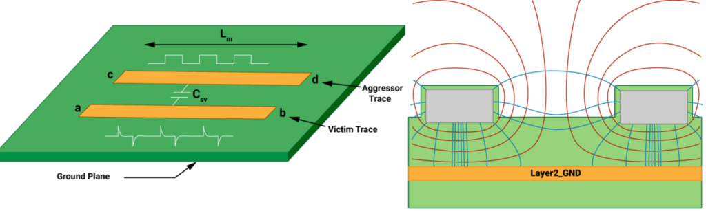
Crosstalk occurs when a signal on an aggressor trace induces unwanted voltage or current on a nearby victim trace through capacitive or inductive coupling. Capacitive crosstalk, dominant at the near end, arises from electric field coupling between traces, while inductive crosstalk affects the far end due to mutual inductance from changing magnetic fields. In high-speed digital design crosstalk scenarios, these effects distort eye diagrams, introduce jitter, and elevate bit error rates. Signal integrity high-speed design relies on minimizing such interference to prevent timing violations and logic errors. For instance, in multi-gigabit interfaces, even small noise pulses can flip data bits or trigger false switching. The relevance intensifies with shrinking geometries and rising frequencies, making crosstalk a primary concern for achieving compliance with performance specifications.
Mechanisms and Causes of Crosstalk
The primary mechanisms stem from electromagnetic fields generated by fast-switching signals propagating along parallel transmission lines. When traces run parallel for extended lengths, the electric field between them creates capacitive coupling, proportional to trace overlap area and inversely to separation distance. Inductive coupling results from loop areas formed by current changes, enhanced by higher di/dt from rapid rise times typical in high-speed signals. Factors like dielectric material properties and reference plane proximity further influence coupling strength. In multilayer boards, coupling can occur both laterally on the same layer and vertically between layers if planes are absent. Rise times below 100 picoseconds exacerbate these effects, as higher frequency components increase field interactions.
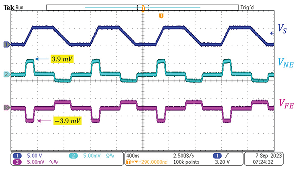
Trace geometry plays a pivotal role, with narrower widths and closer spacing heightening susceptibility. Impedance mismatches along the line can reflect energy, amplifying crosstalk peaks. Ground bounce from simultaneous switching further couples noise through power planes. Engineers observe that forward crosstalk adds to the victim signal, potentially causing overshoot, while backward crosstalk creates glitches at the receiver. These dynamics demand precise modeling during layout planning.
Challenges in Managing High-Speed Digital Design Crosstalk
Densification of PCBs for high-speed applications reduces trace spacing, directly intensifying coupling risks. As edge rates sharpen with advanced technologies, even short parallel sections induce significant noise, challenging traditional spacing rules. Balancing routing density with signal integrity high-speed design constraints often conflicts with size and cost goals. Multilayer stackups introduce inter-layer coupling if reference planes lack sufficient stitching or continuity. Differential pairs, while resilient, still suffer from common-mode to differential-mode conversion under aggressive layouts. Thermal expansions and material variations add variability, complicating predictions.
Measurement challenges persist, as time-domain reflectometry or vector network analyzers require de-embedding for accurate far-end crosstalk assessment. Compliance testing under loaded conditions reveals issues missed in simulations. Supply noise interaction turns crosstalk into systemic problems, affecting clock distribution networks. In dense designs, via transitions create stubs that resonate at frequencies aligning with harmonics, worsening coupling.
Related Reading: Shielding Strategies: Effective Crosstalk Reduction for Sensitive Circuits
Crosstalk Mitigation Strategies and Best Practices
Effective crosstalk mitigation strategies begin with layout optimization, adhering to conservative spacing rules like three times the trace width between singles. IPC-2221 provides guidance on minimum clearances to control coupling in controlled impedance environments. Limit parallel run lengths to less than one-quarter wavelength at the highest frequency component, typically under 1 cm for multi-GHz signals. Route high-speed traces perpendicular on adjacent layers to minimize broadside coupling. Dedicated reference planes adjacent to signal layers offer low-inductance return paths, reducing loop areas.
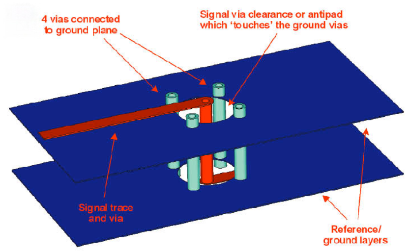
Guard traces, grounded at multiple points, intercept fields between aggressors and victims, though they consume board space. Differential routing preserves balance, inherently rejecting common-mode noise from crosstalk. Controlled impedance matching, per IPC-2221 standards, ensures predictable propagation and minimizes reflections that amplify coupling. Stitching vias along plane edges maintain return current paths, suppressing slot resonances. Pre-layout simulations verify margins before fabrication.
Material selection influences dielectric constant uniformity, aiding consistent coupling reduction. Avoid splitting planes under high-speed nets to prevent return path detours. For vertical coupling, symmetric stackups with plane-signal-plane sequences prove effective. Post-layout reviews focus on length matching within pairs and avoiding right-angle bends that increase radiation.
Advanced Techniques for Signal Integrity High-Speed Design
Beyond basics, active shielding via grounded traces with dense via fences offers superior isolation in critical zones. SerDes channels benefit from equalizer settings compensating for crosstalk-induced ISI. Frequency-domain analysis identifies peak coupling bands for targeted fixes. Hybrid approaches combine microstrip and stripline routing, leveraging enclosed fields in inner layers. IPC-2141A outlines impedance control methods enhancing these strategies. Designers iterate between field solvers and extractions for validation.
Empirical tuning during prototyping uses TDR to measure coupling coefficients, guiding revisions. Multi-board systems require connector pin assignments minimizing adjacent aggressors.
Related Reading: The Impact of Impedance Control on Crosstalk: A Comprehensive Analysis
Conclusion
High-speed digital design crosstalk demands proactive attention through informed layout choices and adherence to proven principles. By implementing spacing rules, robust stackups, and reference planes, engineers significantly enhance signal integrity high-speed design outcomes. Challenges from density and speed persist, but structured mitigation strategies yield reliable boards. Integrating these practices early prevents costly respins and ensures compliance. Future designs will lean on denser interconnects, underscoring the need for vigilant crosstalk control. Mastering these elements positions teams for success in demanding applications.
FAQs
Q1: What causes high-speed digital design crosstalk in PCBs?
A1: High-speed digital design crosstalk arises primarily from electromagnetic coupling between adjacent traces, driven by capacitive electric fields and inductive magnetic fields. Fast rise times and long parallel runs amplify these effects, inducing noise on victim signals. Dielectric variations and absent reference planes exacerbate the issue. Engineers mitigate by increasing spacing and optimizing stackups for better isolation.
Q2: What are effective crosstalk mitigation strategies for signal integrity high-speed design?
A2: Crosstalk mitigation strategies include enforcing 3W spacing, using guard traces, and placing solid ground planes adjacent to signals. Limiting parallel lengths and routing perpendicular on layers reduces coupling. Differential signaling and impedance control further bolster integrity. These practices align with industry guidelines for reliable performance.
Q3: How does PCB stackup impact high-speed digital design crosstalk?
A3: PCB stackup directly influences high-speed digital design crosstalk by defining reference plane proximity and inter-layer distances. Signal-plane-ground sequences minimize broadside coupling, while stitching prevents slot effects. Poor stackups increase inductive loops and field fringing. Optimized designs per standards ensure low crosstalk budgets.
Q4: Why is signal integrity high-speed design critical for crosstalk control?
A4: Signal integrity high-speed design focuses on preserving waveform quality against crosstalk, which introduces jitter and errors at gigabit rates. Without control, systems fail eye mask tests and exhibit BER issues. Proactive strategies like plane referencing maintain margins. This approach supports scalable, high-performance electronics.
References
IPC-2221B — Generic Standard on Printed Board Design. IPC, 2003
IPC-2141A — Design Guide for High-Speed Controlled Impedance Circuit Boards. IPC, 2006
IPC-6012E — Qualification and Performance Specification for Rigid Printed Boards. IPC, 2017
J-STD-001H — Requirements for Soldered Electrical and Electronic Assemblies. IPC, 2018