Introduction
As an electronic hobbyist, you might have built simple circuits with Arduino or Raspberry Pi without worrying much about signal quality. However, when you venture into faster projects like USB interfaces, wireless modules, or even basic Ethernet connections, strange issues like data errors or garbled signals can appear. These problems often stem from PCB impedance mismatches that cause signal reflections. Understanding PCB impedance helps you design reliable boards that perform as expected. This guide explains what PCB impedance is, why impedance control matters, and basic steps for hobbyists to implement it. By the end, you'll have the confidence to specify controlled impedance in your next PCB order.
What Is PCB Impedance?
PCB impedance refers to the characteristic impedance of the conductive traces on a printed circuit board, measured in ohms. It acts like the "resistance" to alternating current signals traveling along the trace, combining effects from inductance and capacitance. In simple terms, imagine a trace as a highway for electrical signals; impedance determines how smoothly high-frequency signals travel without bouncing back. For hobbyists, this becomes relevant when signals switch quickly, such as in digital communications above a few megahertz. Unlike DC resistance, which is steady, impedance varies with frequency and trace geometry. Key types include single-ended impedance for individual traces and differential impedance for paired traces used in balanced signals.
Why Is Impedance Control Important in PCB Design?
Impedance control ensures that the trace impedance matches the source driver's output and the receiving device's input, preventing signal reflections. Reflections occur when a signal encounters a sudden change in impedance, like a narrowing road causing traffic to pile up, leading to distortion, timing errors, or data corruption. For hobbyists working on projects with USB 2.0, SPI buses at high speeds, or RF antennas, uncontrolled impedance can make circuits unreliable or fail entirely. Proper control maintains signal integrity, reduces electromagnetic interference, and improves overall board performance. In high-speed designs, even small mismatches amplify problems over longer trace lengths. Standards like IPC-2141 provide guidelines to achieve consistent impedance across manufacturing variations.
Without control, hobbyist prototypes might work in testing but fail in real use due to manufacturing tolerances in trace width or material properties. Impedance mismatches also increase power consumption from ringing signals. By specifying control, you ensure your PCB fabricator adjusts the design to hit target values, typically 50 ohms for single-ended or 90-100 ohms differential. This practice is crucial as hobby projects evolve toward more complex, faster electronics.
PCB Impedance Explained Simply: The Basics
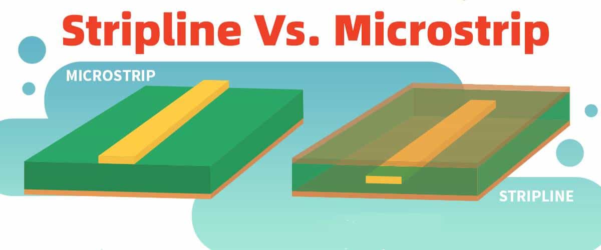
At its core, PCB impedance arises from the transmission line formed by a trace and its reference plane, governed by the formula involving inductance per unit length and capacitance per unit length. Wider traces lower impedance because they increase capacitance to the nearby ground plane; narrower traces raise it by reducing capacitance. The dielectric material between layers, with its dielectric constant (Er around 4 for common FR-4), heavily influences capacitance and thus impedance. Thicker dielectrics increase impedance by spacing the trace farther from the plane. For hobbyists, microstrip traces (signal on outer layer over ground plane) are common and easier to route, while striplines (embedded between planes) offer better shielding but require symmetric stackups.
Frequency plays a role too: at low speeds, like audio signals, impedance mismatches are negligible, but above 100 MHz, they matter. IPC-2221 outlines generic design rules that indirectly support impedance considerations through layer stackup and spacing. Hobbyists can think of it as tuning a guitar string: the right width, height, and material tension (geometry and dielectric) produce the desired "pitch" or ohm value.
Basic PCB Impedance Control for Hobbyists
Start with your PCB stackup, which defines layer thicknesses and materials; request a 4-layer board with ground planes adjacent to signal layers for stable reference. Use consistent trace widths across coupled pairs for differential signals, maintaining equal spacing to ground. Specify target impedances in fab notes, like "50 ohm single-ended microstrip on layers 1 and 4, +/-10% tolerance." Fabricators use field solvers to adjust etch widths based on their process, often providing an impedance table after review. For hobbyists, aim for standard values: 50 ohms for RF/USB, 90 ohms differential for LVDS. Avoid vias in critical lines or use back-drilled ones to minimize stubs that disrupt impedance.
Test control post-fabrication with a time-domain reflectometer (TDR) if available, or scope signals for ringing. Manufacturing tolerances like etch variation (+/-10-20%) necessitate control specs. Keep traces short and away from edges to avoid fringing fields. In multilayer boards, plane splits can cause impedance jumps, so route over solid ground.
Common Challenges and Troubleshooting in Hobbyist Designs
Hobbyists often face impedance issues from thin 2-layer boards lacking nearby ground planes, leading to high, unpredictable values. Solution: upgrade to 4-layers for better control without much cost increase. Another pitfall is inconsistent dielectric thickness from fab variations; always request controlled stackup. Differential pairs may skew if lengths or widths differ, causing common-mode noise; use length-matching tools in your design software. Signal crosstalk from adjacent traces erodes integrity; space them at least 3x dielectric thickness apart.
If signals ring on oscilloscope, suspect mismatch: shorten traces or add series resistors for termination. For RF hobby projects, simulate roughly with online calculators before fab. Troubleshooting starts with verifying fab's impedance report against your spec.
Conclusion
Mastering PCB impedance demystifies high-speed design for hobbyists, turning potential frustrations into reliable prototypes. From understanding what PCB impedance is to implementing basic control via stackup and specs, these steps elevate your projects. Prioritize impedance matching to avoid reflections, especially as speeds increase. Reference standards like IPC-2141 for best practices, and always communicate clearly with fabricators. With practice, controlled impedance becomes a standard part of your workflow, enabling ambitious electronics like custom WiFi modules or data loggers. Start simple, test iteratively, and watch your boards perform flawlessly.
FAQs
Q1: What is PCB impedance in simple terms?
A1: PCB impedance is the opposition traces offer to high-frequency signals, determined by trace geometry and materials. It ensures signals travel without distortion, much like a matched pipe for water flow. For hobbyists, think of it as setting the right "size" for fast data lines to prevent errors. Understanding PCB impedance for hobbyists starts with recognizing its role in USB or SPI reliability.
Q2: Why is impedance control important in PCB for beginner projects?
A2: Impedance control prevents signal reflections that cause data errors in high-speed hobby circuits like Ethernet or Bluetooth. Without it, prototypes may work sporadically due to manufacturing variations. It maintains clean waveforms, reducing debug time. Basic PCB impedance control via fab specs ensures consistency, vital for reliable performance.
Q3: How do you achieve basic PCB impedance control as a hobbyist?
A3: Specify target ohms (e.g., 50 single-ended) and layer stackup in your Gerber files' notes. Use 4-layer boards with ground planes next to signals for stability. Request fab verification via TDR. Adjust trace widths per their calculator feedback. This simple process handles most hobby needs without advanced tools.
Q4: When does a hobbyist PCB need impedance control?
A4: Control is essential for traces longer than 1/10 wavelength of your signal frequency, like USB over 10 cm or clocks above 50 MHz. Low-speed analog or power lines often skip it. PCB impedance explained simply: match it when signals distort on scope. Start with high-speed digital interfaces in your projects.
References
IPC-2141A — Design Guide for High-Speed Controlled Impedance Circuit Boards. IPC
IPC-2221B — Generic Standard on Printed Board Design. IPC
IPC-6012E — Qualification and Performance Specification for Rigid Printed Boards. IPC, 2017


