Introduction
As electronic hobbyists dive into designing their own printed circuit boards, they often encounter challenges with high-speed signals in projects like microcontrollers, sensors, and wireless modules. Signal integrity becomes crucial when signals travel across traces at faster rates, potentially leading to errors or system failures. This guide breaks down the signal integrity definition PCB in simple terms, explores common pitfalls, and offers practical steps to ensure reliable performance. Whether you are prototyping a drone controller or a home automation board, understanding these basics will save time and frustration. By following straightforward rules, even beginners can achieve professional results without advanced tools.
Hobby projects often start simple, but adding features like Ethernet or DDR memory introduces signal integrity concerns early. Signals can degrade due to unintended interactions within the PCB layout itself. Recognizing this upfront allows for proactive design choices that enhance reliability.
What Is Signal Integrity in PCBs?
The signal integrity definition PCB refers to the ability of an electrical signal to maintain its intended shape, voltage levels, and timing as it propagates from the driver to the receiver across the board. In essence, it measures how well the signal resists degradation caused by the PCB's physical structure and materials. Poor signal integrity results in distorted waveforms, bit errors, or complete communication breakdowns, especially in digital circuits operating above a few megahertz. For hobbyists, this concept is key when integrating components like FPGAs or high-speed USB interfaces. Standards like IPC-2221 provide foundational guidelines for designing traces that preserve signal quality.
Hobby projects often start simple, but adding features like Ethernet or DDR memory introduces signal integrity concerns early. Signals can degrade due to unintended interactions within the PCB layout itself. Recognizing this upfront allows for proactive design choices that enhance reliability.
Why Signal Integrity Matters for Electronic Hobbyists
Electronic hobbyists increasingly build boards with faster processors and communication protocols, making signal integrity issues in PCBs a frequent roadblock. A small glitch, such as crosstalk between traces, can cause intermittent failures that are hard to debug during testing. Reliable signal integrity ensures your project works consistently, from bench prototyping to real-world deployment. It directly impacts data throughput, power efficiency, and electromagnetic compliance in compact designs. Ignoring it leads to respins, wasted components, and delayed progress.
In hobbyist contexts, where budgets are tight and iterations manual, strong signal integrity reduces troubleshooting hours. Projects involving IoT devices or audio interfaces benefit most, as clean signals prevent noise-induced artifacts. Ultimately, mastering these principles elevates homemade boards to match commercial quality.
Common Signal Integrity Issues in PCBs
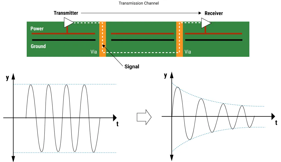
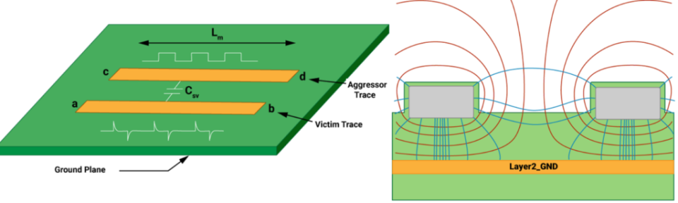
Signal integrity issues in PCBs manifest in several ways, starting with reflections that occur when signal impedance mismatches cause waves to bounce back. Crosstalk happens when electromagnetic fields from one trace induce noise on a nearby one, corrupting data. Attenuation gradually weakens high-frequency components over long traces, flattening signals. Ground bounce arises from simultaneous switching of multiple outputs, creating voltage fluctuations on ground planes. Timing skew, or unequal propagation delays, disrupts synchronized signals like clocks.
These problems compound in multilayer boards common among hobbyists experimenting with complexity. Beginners might notice erratic behavior, such as random resets or garbled serial data. Early identification through basic simulations or oscilloscope checks prevents escalation.
Root Causes of Signal Integrity Problems
Impedance discontinuities top the list of causes, often from abrupt trace width changes, vias, or connector transitions. Poor return path design, like missing ground planes under signals, increases loop inductance and noise pickup. Dielectric variations in the PCB material affect propagation speed inconsistently across layers. Excessive via count introduces stubs that reflect energy back. Component placement far from drivers stretches traces, amplifying losses.
Hobbyists frequently overlook stackup planning, where layer sequencing impacts coupling. Manufacturing tolerances, though minimal in standard processes, can shift characteristic impedance slightly. Addressing these at the schematic stage sets a solid foundation.
Basic Signal Integrity Rules for PCB Design
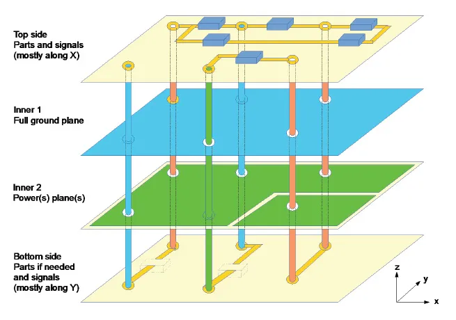
Adhering to basic signal integrity rules simplifies design for beginners. First, calculate and control trace impedance to match driver and receiver specs, typically 50 or 100 ohms for single-ended or differential pairs. Route high-speed signals on inner layers with adjacent ground planes for better shielding. Maintain consistent trace widths and minimize bends to avoid discontinuities. Space parallel traces adequately to reduce crosstalk, aiming for at least three times the trace width separation.
Keep clock lines short and symmetric, avoiding splits that cause skew. Place decoupling capacitors close to power pins to stabilize supply voltage. These rules align with IPC-6012 performance specifications, ensuring boards meet quality benchmarks. Hobbyists can apply them using free design software's built-in calculators.
Use solid ground pours rather than grids for low-impedance returns. Avoid routing signals over splits in planes. Test rules with design rule checks before fabrication.
Practical Best Practices to Ensure Signal Integrity
Start with a well-planned stackup: alternate signal and plane layers for optimal coupling. For differential pairs, ensure equal lengths and tight spacing to preserve common-mode rejection. Minimize vias by strategic component placement; use blind or buried vias if layers allow. Add series termination resistors near drivers for source matching in point-to-point links. Guard traces with ground lines on both sides for sensitive analog signals.
During layout, prioritize critical nets first, then fill with others. Simulate simple cases with free tools to verify eye openings. Post-layout, review for length mismatches under 1% for high-speed buses. These practices form a signal integrity checklist hobbyists can follow iteratively.
In assembly, follow J-STD-001 guidelines for soldering to avoid introducing defects like cold joints that worsen noise. Prototype on smaller boards to validate before scaling.
Signal Integrity Checklist for Beginners
A practical signal integrity checklist streamlines reviews:
- Verify trace impedance matches requirements using stackup calculators.
- Check minimum spacing between high-speed traces: at least 3x height over ground.
- Confirm differential pair lengths within tolerance, typically <0.5 mm skew.
- Ensure ground planes are unbroken under signals with no splits.
- Place bypass capacitors <1 cm from IC power pins.
- Limit vias per net to essentials; stub length <1/10 wavelength.
- Review bend angles: 45 degrees or smooth curves only.
Run this before Gerber export. It catches 80% of issues early. Adjust based on frequency: stricter for GHz signals.
Troubleshooting Common Issues
When signals falter, scope the nets: look for ringing indicating reflections. Adjust termination if overshoot appears. For crosstalk, increase spacing or add shielding. Eye diagrams, even hand-drawn approximations, reveal closure from jitter. Iterate layouts incrementally.
Hobbyists benefit from breadboard validation first. Log changes systematically.
Conclusion
Signal integrity in PCBs demystified reveals it as a manageable aspect of design through understanding definitions, issues, rules, and checklists. Beginners armed with these insights produce robust boards for ambitious projects. Consistent application yields reliable, high-performance results without deep expertise. Prioritize impedance control, clean routing, and verification for success. As your skills grow, explore simulations for even finer tuning.
FAQs
Q1: What is the signal integrity definition PCB in simple terms?
A1: Signal integrity definition PCB describes how well electrical signals stay true to their original form while traveling across board traces. Degradation from reflections or noise leads to errors in digital communication. For hobbyists, it ensures clocks and data lines function correctly at speed. Follow basic rules like impedance matching to maintain it.
Q2: What are the main signal integrity issues in PCBs for beginners?
A2: Signal integrity issues in PCBs include reflections from mismatches, crosstalk between traces, and attenuation over distance. Ground bounce from power fluctuations also disrupts logic levels. Hobbyists see these as erratic behavior in prototypes. Mitigate with ground planes and proper spacing for cleaner signals.
Q3: What are basic signal integrity rules every hobbyist should know?
A3: Basic signal integrity rules involve controlling trace impedance, using ground planes adjacent to signals, and matching lengths for pairs. Avoid sharp bends and excess vias. Space traces to cut crosstalk. These prevent common failures in high-speed designs.
Q4: How do I use a signal integrity checklist in my PCB project?
A4: A signal integrity checklist verifies impedance, spacing, skew, and plane integrity before fab. Check decoupling placement and via counts too. It catches issues early, saving respins. Tailor to your clock rates for best results.
References
IPC-2221 - Generic Standard on Printed Board Design. IPC
IPC-6012E - Qualification and Performance Specification for Rigid Printed Boards. IPC, 2017
J-STD-001G - Requirements for Soldered Electrical and Electronic Assemblies. IPC/JEDEC, 2011