Why Choose KiCad for Wearable Electronic Projects?
KiCad stands out as an exceptional, freely available, and open-source solution for printed circuit board (PCB) design, making it a prime choice for wearable electronics. Its robust feature set encompasses schematic capture, detailed PCB layout editing, and 3D visualization capabilities. Crucially, unlike many proprietary tools, KiCad imposes no restrictions on board dimensions or the number of layers, which is highly beneficial for both hobbyists and seasoned engineers tackling wearable devices.
Wearable gadgets inherently demand designs that are small, often flexible, and feature precise component placement. KiCad’s versatile toolkit is well-equipped to manage these specific requirements effectively. Furthermore, a vibrant and active community supports KiCad, offering a wealth of resources, component libraries, and plugins, ensuring ample assistance for developing complex and intricate designs.
What Unique Challenges Do Wearable PCB Designs Present?
Miniaturization and Power Considerations
Before delving into the design process, it's vital to grasp the distinct obstacles involved in creating PCBs for wearable technology. These devices must be exceedingly small, lightweight, and frequently flexible to ensure wearer comfort. Size is a paramount constraint; for instance, smart rings or fitness bands often require PCB layouts under 30mm x 30mm. Power efficiency is equally critical, demanding designs that achieve minimal energy consumption, with targets often below 10mA in standby modes to extend battery life.
Flexibility, Signal Integrity, and Thermal Management
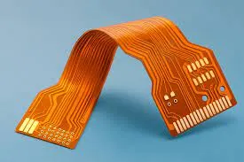
Many wearables integrate flexible PCBs or rigid-flex PCBs to conform to the body's contours, necessitating specific design rules. Maintaining signal integrity is another challenge; high-frequency signals, such as 2.4 GHz Bluetooth, require meticulous routing in confined spaces to prevent interference. Lastly, heat dissipation must be managed effectively within enclosed designs that are in direct contact with skin, typically by keeping component temperatures below 40°C. KiCad provides the tools to address these challenges systematically.
Getting Started with Your First KiCad Wearable Project
Software Installation and Core Components
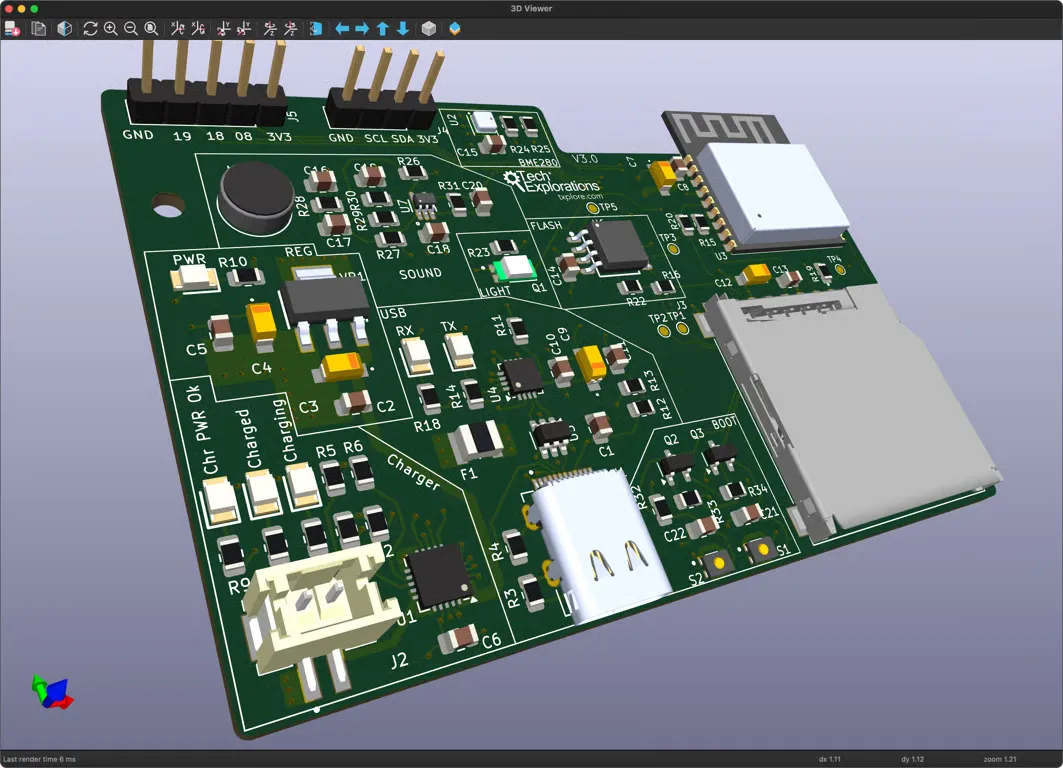
To begin your journey with KiCad, first download and install the software from its official website. It supports Windows, macOS, and Linux platforms. Once installed, familiarize yourself with KiCad's primary modules: Eeschema for schematic capture, Pcbnew for PCB layout, and the 3D Viewer for visualizing your design. This guide assumes a foundational understanding of electronics; for beginners, KiCad's documentation offers comprehensive learning resources.

Project Setup and Initial Schematic Design
Start by establishing a new project within KiCad, perhaps for a basic fitness tracker incorporating a microcontroller, various sensors, and Bluetooth connectivity. The schematic serves as the blueprint for your rigid flex PCB. In the schematic editor, you will add components—such as an ARM Cortex-M0 microcontroller, a heart rate sensor, and a Bluetooth module—from KiCad's extensive libraries or by creating custom symbols. Connect these components with wires, ensuring accurate power and ground connections. For wearable applications, incorporate a lithium-ion battery input, typically 3.7V, along with essential protection circuitry. After assigning reference designators, run an Electrical Rules Check (ERC) to identify any potential errors.
Key Steps in KiCad PCB Layout for Wearables
Assigning Footprints and Defining Board Dimensions
After completing your schematic, the next step involves linking each logical component to its physical footprint. Footprints dictate the physical appearance of components on the PCB, including pad sizes and shapes. Use KiCad’s "Assign Footprints" utility to match schematic symbols with library footprints, prioritizing compact surface-mount device (SMD) packages like 0402 or 0201 for passive components to conserve space. If a unique footprint is needed, KiCad’s Footprint Editor allows for custom creations. Subsequently, move to the PCB layout editor (Pcbnew) to define the board's dimensions. For a wristband sensor, this might mean a compact 25mm x 20mm outline, drawn on the "Edge.Cuts" layer.
Component Placement and Trace Routing
Strategic component placement is critical for wearables. Position the microcontroller centrally, with sensors located near the board's edge for optimal skin contact. Isolate high-frequency components, such as Bluetooth modules, from sensitive analog parts to mitigate interference. Route power and ground traces first, ideally utilizing a ground plane to minimize noise. For high-speed signals (e.g., I2C or SPI, operating at 400 kHz to 1 MHz), keep traces short and use 45-degree angles instead of sharp 90-degree bends. Regularly perform a Design Rules Check (DRC) to confirm that clearances meet manufacturing specifications. For space-constrained wearable PCBs, consider a 4-layer board configuration to separate power, ground, and signal traces, reducing crosstalk and allowing for a thinner total board thickness (e.g., 0.8mm).
Advanced Considerations for Wearable PCB Designs
Flexible Boards, Antenna Integration, and Thermal Management
Wearable electronics frequently demand specialized design elements. For flexible boards, define bendable zones within your layout using KiCad’s custom board outline capabilities and specify thinner substrates like 0.1mm polyimide in your design documentation. When integrating wireless connectivity, such as Bluetooth or Wi-Fi, either embed a trace antenna directly into the design or allocate sufficient space for a chip antenna, ensuring at least a 5mm clearance to prevent signal degradation at 2.4 GHz. Thermal management is also crucial; incorporate thermal vias under heat-generating components to dissipate heat effectively, aiming to keep skin-contact areas below 38°C. KiCad's 3D viewer is invaluable for visualizing how the PCB integrates into its enclosure, ensuring comfortable fit and preventing component protrusion.
Manufacturing File Generation and Iterative Testing
Once the design is finalized, generate the necessary manufacturing files using KiCad’s "Plot" feature to export Gerber files for each layer (copper, silkscreen, solder mask) and a drill file for vias and holes. Review these files with KiCad’s Gerber viewer to catch any potential errors. A Bill of Materials (BOM) detailing all components, part numbers, and quantities must also be generated for assembly. After manufacturing, thorough testing of the wearable PCB is essential. Verify power delivery, sensor accuracy, and wireless connectivity range. Should issues arise, KiCad's integrated schematic and layout editors facilitate efficient design iteration, allowing for adjustments like modifying trace lengths, adding decoupling capacitors, or repositioning components to optimize performance.
Final Tips for Mastering Wearable PCB Design with KiCad
To successfully create efficient wearable electronics using open-source tools like KiCad, consider these additional insights. Actively utilize KiCad’s extensive libraries of pre-made symbols and footprints to streamline your design process and keep them updated for the latest components. While KiCad itself doesn't offer built-in simulation, integrate with external open-source tools to simulate circuits before layout, especially to ensure signal integrity for high-frequency applications. Engage with the KiCad community through forums and user groups for specialized advice on wearable challenges, such as designing for water resistance standards like IP67. Above all, strive for simplicity; in wearable design, prioritizing essential features over unnecessary components helps reduce size, power consumption, and overall complexity.
Designing PCBs for wearable electronics presents a rewarding challenge, and KiCad, as a robust open-source solution, provides all the necessary tools. This tutorial has covered the fundamental aspects, from schematic creation to compact board layouts and manufacturing file generation, all specifically tailored for wearable applications. By diligently addressing constraints related to size, power efficiency, and signal integrity, you can develop innovative devices that meet contemporary demands. Embrace KiCad for your next wearable project and leverage its adaptability and community support to bring your concepts to fruition. With persistent practice, you will master the art of crafting efficient and reliable PCBs for the rapidly expanding field of wearable technology.


