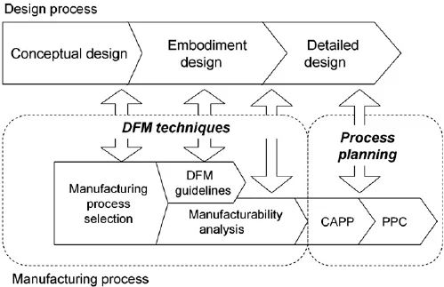
Introduction
In the competitive landscape of electronics engineering, a thorough PCB DFM review stands as a critical step before production begins. Design for manufacturability PCB practices integrate manufacturing constraints directly into the design phase, minimizing defects and production delays. Engineers often overlook these checks, leading to costly respins and extended timelines. By conducting a systematic PCB DFM review, teams can identify potential issues early, ensuring boards meet performance goals while staying within budget. This process not only enhances yield rates but also aligns designs with factory capabilities for smoother transitions to assembly.
The stakes are high in modern PCB projects, where complexity from high-density interconnects and fine-pitch components amplifies risks. A well-executed design for manufacturability PCB approach reduces material waste and labor costs by up to significant margins through proactive optimization. For electric engineers, mastering PCB DFM review means bridging the gap between innovative designs and reliable production outcomes. This article explores the principles, checklists, and best practices to streamline your workflow.
What Is PCB DFM Review and Why It Matters
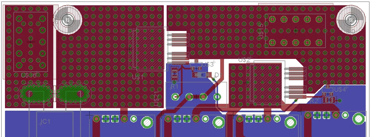
PCB DFM review refers to the systematic evaluation of a printed circuit board design against manufacturing capabilities and constraints. It encompasses checks for fabricability, assemblability, and testability, ensuring the design translates seamlessly into production. This review typically occurs after schematic capture and layout but before Gerber file release, involving collaboration between designers and fabrication experts. Core elements include verifying layer stackups, trace geometries, and drill patterns to prevent issues like shorts or opens during fabrication.
The relevance of design for manufacturability PCB cannot be overstated in today's fast-paced industry. Poor DFM leads to engineering change orders, which inflate costs and delay market entry. Factories report that early DFM interventions cut scrap rates substantially by addressing non-manufacturable features upfront. Compliance with standards like IPC-2221, which outlines generic requirements for printed board design, provides a foundation for these reviews. Engineers benefit from higher first-pass yields, reducing the need for multiple prototypes.
Moreover, PCB DFM review fosters cost efficiency by optimizing material usage and process steps. For instance, balanced copper distribution prevents warpage, a common failure mode in multilayer boards. In high-volume production, these savings compound, making DFM a strategic imperative rather than an optional step. Electric engineers who prioritize this review gain a competitive edge through reliable, cost-effective boards.
Key Technical Principles of Design for Manufacturability in PCB
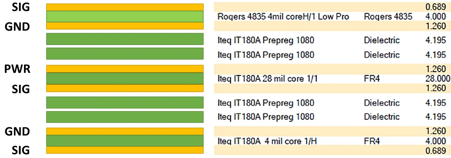
Effective design for manufacturability PCB hinges on foundational principles that govern material selection and board construction. Laminate choices must consider thermal expansion coefficients to match component requirements, avoiding stress during reflow soldering. Stackup design demands symmetry in copper layers to minimize warpage, with core and prepreg thicknesses aligned for uniform thickness control. Factory processes favor standard panel sizes and thicknesses, which streamline handling and tooling. Adhering to these principles ensures dimensional stability across the production run.
Routing guidelines form another pillar of PCB DFM review. Minimum trace widths and spacings must accommodate etching tolerances, typically scaling with board class and copper weight. High-speed signals require controlled impedance, but manufacturability dictates avoiding acute angles that cause undercuts during etching. Vias should feature adequate annular rings to withstand drill breakout, with non-functional pads tented to prevent solder wicking. These rules prevent electrical failures while supporting high yields.
Pad and land pattern geometries directly impact assembly success. Solder joints rely on proper pad sizes relative to component leads, preventing bridging or insufficient fillet formation. Clearances between pads and traces avoid solder mask bridging during application. For fine-pitch devices, expanded pads compensate for placement tolerances inherent in pick-and-place machines. Visual inspection confirms these features meet acceptability criteria before production.
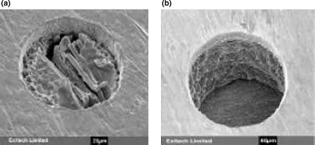
Drill and plating processes demand precise hole sizing and aspect ratios. Mechanical drills have size increments and tolerances that influence registration accuracy. Plated through-holes require sufficient copper thickness for conductivity, with back-drilling used for signal integrity in dense designs. Panelization strategies, including v-scoring or tab routing, must account for depanelization stresses. These considerations ensure reliable interconnections without barrel cracks.
Surface finishes like HASL or ENIG influence solderability and shelf life, but DFM prioritizes uniformity to avoid defects like black pad. Silkscreen and solder mask alignments prevent misregistration that could expose traces. Copper balance across layers reduces plating variations, promoting consistent finish deposition. By embedding these principles, engineers create robust designs primed for manufacturing.
PCB Manufacturing Checklist: Best Practices for DFM Success
A comprehensive PCB manufacturing checklist serves as the backbone of any effective PCB DFM review. Start with file integrity: ensure Gerbers, drill files, and stackup diagrams match the design intent, with ODB++ or IPC-2581 formats preferred for data fidelity. Verify units consistency and aperture lists to eliminate scaling errors. Cross-check netlists against schematics to catch routing discrepancies early.
Layer-specific checks include copper pour symmetry and trace-to-edge clearances. Minimum distances from board outline prevent etching exposure, while inner layer alignments avoid misalignment during lamination. Solder mask expansion rules protect traces without encroaching on pads, and via tenting specifications enhance reliability. Reference IPC-6012 for qualification specs on rigid boards to validate these features.
Component and assembly considerations extend the checklist. Footprint libraries must align with land pattern standards, incorporating courtyard keep-outs for automated placement. Fiducials provide registration marks for precision alignment, with at least three per panel. Thermal pads for power devices require via stitching to dissipate heat effectively. These practices minimize reflow defects and enhance testability.
Fabrication tolerances guide final validations. Annular ring requirements scale with drill size, ensuring breakout resistance. Aspect ratios for vias stay below 10:1 to guarantee plating uniformity. Board outline features like chamfers aid handling, while scoring lines facilitate clean depanelization. Simulate warpage using stackup calculators to predict bow and twist limits.
Test point placement rounds out the checklist, with accessible probes for in-circuit testing. Non-functional elements like test coupons validate material properties post-fabrication. Document all deviations with engineering rationale for traceability. Implementing this PCB manufacturing checklist systematically slashes iteration cycles and boosts factory throughput.
Common DFM Pitfalls in PCB Design and Proven Solutions
Despite best efforts, certain DFM pitfalls persist in PCB design review. Asymmetric stackups often cause warpage exceeding 0.75% of board dimension, leading to assembly failures. Solution lies in mirroring copper densities and using balanced cores, verified through 3D modeling. Factories detect this via shadow moire analysis, but prevention starts in design.
Trace necking or insufficient spacing results in etching shorts, particularly on inner layers. Maintain minimums per copper weight, with acid traps avoided through teardrop connections. Solder mask slivers between pads thinner than 0.1 mm bridge during printing, so expand clearances accordingly. These fixes align with soldering requirements in J-STD-001.
Via-in-pad designs without fill specifications cause solder entrapment or planarity issues. Specify plugged or filled vias early, matching assembly processes. Oversized drills erode annular rings below minimums, compromising reliability; use aspect-ratio calculators for optimization. Troubleshooting these elevates design maturity.
Component orientation inconsistencies complicate assembly programming. Standardize polarity markings and fiducial placement for machine vision. Ignoring panelization leads to fragile tabs or stress concentrations during routing. Opt for optimized arrays with robust breakaways. Addressing these pitfalls through iterative DFM review ensures production success.
Conclusion
PCB DFM review transforms potential design flaws into manufacturable realities, directly impacting costs and timelines. By embracing design for manufacturability PCB principles and a rigorous PCB manufacturing checklist, electric engineers secure higher yields and reliability. Key practices like stackup symmetry, precise routing, and tolerance adherence form the core of success. Integrating standards guidance elevates outcomes across projects. Prioritize these steps to streamline from concept to production.
FAQs
Q1: What does a PCB DFM review entail?
A1: A PCB DFM review systematically checks design files against fabrication and assembly constraints. It verifies trace widths, clearances, stackups, and drill patterns for manufacturability. Collaboration with factories identifies issues like annular ring deficiencies early. This process, guided by standards, prevents costly respins and ensures high yields. Expect 1-2 days for thorough analysis on complex boards.
Q2: How does design for manufacturability PCB reduce production costs?
A2: Design for manufacturability PCB optimizes features like copper balance and standard drill sizes to minimize waste and process steps. It avoids iterations by catching warpage or bridging risks upfront. Factories achieve better throughput with compliant designs, lowering per-unit expenses. Engineers save on prototypes, focusing resources on innovation instead.
Q3: What are must-have items in a PCB manufacturing checklist?
A3: Essential PCB manufacturing checklist items include Gerber netlist verification, solder mask expansion, via annular rings, and fiducial placement. Check stackup symmetry and board outline clearances too. Validate pad-to-trace spacing and thermal reliefs for assembly. These confirm design-fabrication alignment before production.
Q4: Why reference standards in PCB DFM review?
A4: Standards provide proven benchmarks for tolerances and processes in PCB DFM review. They ensure consistency across suppliers, reducing variability. For example, they define minimum spacings and plating thicknesses for reliability. Compliance builds trust and facilitates quality audits.
References
IPC-2221B — Generic Standard on Printed Board Design. IPC, 2003
IPC-6012E — Qualification and Performance Specification for Rigid Printed Boards. IPC, 2017
J-STD-001G — Requirements for Soldered Electrical and Electronic Assemblies. IPC, 2011