Why is Dielectric Thickness Important for PCB Impedance?
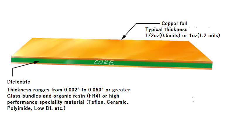
In the world of printed circuit board (PCB) design, understanding the interplay between dielectric thickness and impedance is fundamental for creating high-performance electronics. Dielectric thickness refers to the insulating material's height that separates conductive layers within a PCB, commonly composed of substances like FR-4 with a specific dielectric constant (often between 4.2 and 4.5 at 1 MHz). This physical dimension directly impacts the characteristic impedance of a signal trace, which dictates how electrical signals propagate through the circuit.
The characteristic impedance, measured in ohms, is a critical factor influencing signal integrity, especially in high-speed digital and radio frequency (RF) applications. Any mismatch in impedance can lead to signal reflections, data errors, and a degradation in overall circuit performance. Therefore, PCB engineers must meticulously consider and control dielectric thickness to ensure optimal signal transmission and prevent unwanted signal behavior.
How Does Dielectric Thickness Affect Trace Impedance?
The relationship between the dielectric layer's thickness and the trace impedance is a core principle in PCB design. Generally, an increase in the dielectric thickness leads to a rise in the characteristic impedance of a trace, while a reduction in thickness results in lower impedance. This dynamic occurs because the dielectric layer's height directly influences the distribution of the electric field between the signal trace and its accompanying ground plane.
Illustrating the Impact of Thickness
Consider a common "microstrip" configuration, where a signal trace resides on the outer surface of the PCB, with a ground plane beneath it. If the dielectric thickness is increased—for instance, from 0.2 mm to 0.4 mm—the impedance could shift from a typical 50 ohms to around 65 ohms, assuming other factors like trace width (e.g., 0.3 mm) and dielectric constant (e.g., 4.3) remain constant. This happens because a thicker dielectric reduces the capacitance per unit length between the trace and the ground, consequently increasing the impedance. Conversely, a thinner dielectric heightens capacitance, which in turn lowers the impedance. Engineers must carefully balance these parameters to achieve specific impedance targets, such as 50 ohms for RF circuits or 100 ohms for differential pairs in high-speed digital systems.
What Does "Controlled Impedance" Mean in PCB Design?
Controlled impedance is a design practice where PCB traces are engineered to maintain a specific, consistent characteristic impedance. This precision is vital for high-speed circuits to ensure signals travel without experiencing distortion or reflections. Applications such as USB, HDMI, Ethernet, and various RF systems heavily rely on controlled impedance to guarantee reliable data transmission and optimal performance, as even slight impedance variations can cause significant issues.
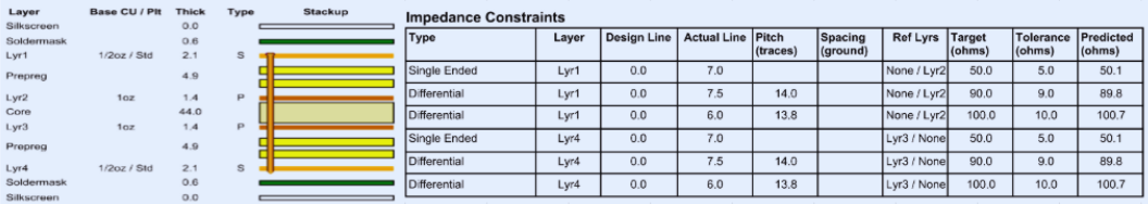
To achieve controlled impedance, designers meticulously select materials, define precise trace dimensions, and rigorously manage dielectric thickness. For example, many high-speed single-ended traces target an impedance of 50 ohms. Reaching this goal demands accurate calculations and often requires specialized manufacturing processes to uphold strict tolerances on both dielectric thickness and the overall geometry of the traces.
How Do Microstrip Traces Influence Impedance?
Microstrip is a widely adopted PCB trace arrangement where the conductor is situated on an external layer of the board, isolated from an underlying ground plane by a dielectric layer. The impedance of a microstrip trace is determined by several factors, including the trace's width, the thickness of the dielectric material, and the dielectric constant of that material. Engineers can estimate this relationship using standard formulas or specialized online calculators.
Calculating Microstrip Impedance
A common formula used to approximate microstrip impedance (Z₀) is:
Z₀ = (87 / √(εᵣ + 1.41)) * ln(5.98 * H / (0.8 * W + T))
Here, Z₀ represents the characteristic impedance in ohms, εᵣ is the dielectric constant of the material (e.g., 4.3 for FR-4), H is the dielectric thickness in mils (e.g., 8 mils), W is the trace width in mils (e.g., 6 mils), and T is the trace thickness in mils (e.g., 1.4 mils for 1 oz copper). For instance, a design with an 8-mil dielectric thickness, 6-mil trace width, 1.4-mil trace thickness, and a dielectric constant of 4.3 might yield an impedance close to 50 ohms. If the dielectric thickness were increased to 10 mils, the impedance would rise to approximately 55 ohms, clearly demonstrating the direct influence of dielectric thickness. Engineers frequently employ simulation software or online resources to refine these calculations, ensuring accuracy for specific board materials and stackups. Prototyping and validation are also crucial steps to confirm that the calculated impedance aligns with actual performance.
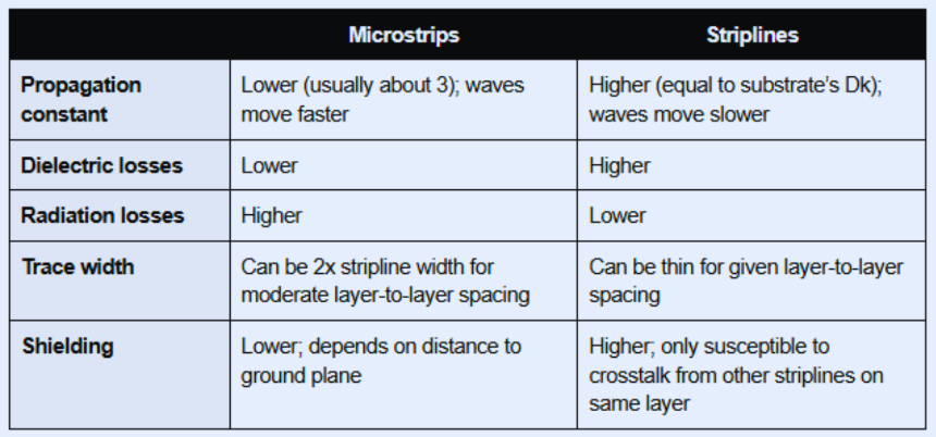
What Sets Stripline Impedance Apart from Microstrip?
Unlike microstrip, a stripline configuration embeds the signal trace between two ground planes, completely encapsulating it within dielectric material. This arrangement offers superior shielding against external interference, making it particularly suitable for high-frequency applications. However, calculating stripline impedance is generally more complex due to the presence of dielectric layers both above and below the trace.
Stripline Impedance Formula
An approximate formula for stripline impedance (Z₀) is:
Z₀ = (60 / √εᵣ) * ln(1.9 * B / (0.8 * W + T))
In this formula, Z₀ denotes the characteristic impedance in ohms, εᵣ is the dielectric constant, B is the total dielectric thickness between the two ground planes in mils, W is the trace width in mils, and T is the trace thickness in mils. For example, a design featuring a total dielectric thickness (B) of 20 mils, a trace width of 5 mils, a trace thickness of 1.4 mils, and a dielectric constant of 4.3 might result in an impedance around 50 ohms. Increasing B to 25 mils could elevate the impedance to roughly 53 ohms, again highlighting the impact of dielectric thickness. Stripline designs typically exhibit lower impedance than microstrip for an equivalent dielectric thickness, primarily due to the increased capacitance provided by having ground planes on both sides. This characteristic often makes stripline the preferred choice for applications demanding stringent impedance control and minimal signal interference.
Practical Steps for Accurate PCB Impedance Calculation
Achieving precise PCB impedance calculations is crucial for successful controlled impedance designs. Here are practical steps and valuable tips to guide engineers through this process:
Begin by identifying the exact impedance required for your application, such as 50 ohms for single-ended RF signals or 100 ohms for differential pairs in high-speed digital circuits. Next, select a dielectric material with a well-defined dielectric constant; FR-4 (with εᵣ of 4.2 to 4.5) is common for standard designs, while high-frequency applications might benefit from materials like Rogers, which have lower dielectric constants (e.g., 3.0 to 3.5). Collaborate closely with your PCB manufacturer to finalize the layer stackup, ensuring that dielectric thicknesses between layers are configured to meet your target impedance.
Utilize specialized online calculators or advanced simulation software, inputting parameters such as trace width, dielectric thickness, and dielectric constant. These tools offer rapid estimates for both microstrip and stripline configurations. After manufacturing, validate your calculations using a Time Domain Reflectometer (TDR) to measure the actual impedance of the traces and compare it against your design targets. Be prepared to adjust trace widths or dielectric thicknesses in subsequent revisions if necessary. It’s also important to remember that manufacturing tolerances can impact impedance; a ±10% variation in dielectric thickness, for instance, can shift impedance by a few ohms, potentially causing signal integrity issues in sensitive circuits. Therefore, always specify tight tolerances for controlled impedance designs and maintain open communication with your PCB fabricator.
Best Practices for Designing Controlled Impedance PCBs
Designing a PCB with controlled impedance demands meticulous attention to detail and adherence to established best practices. These guidelines are crucial for ensuring successful outcomes:
First, strive to maintain a consistent dielectric thickness across the entire board. Any variations can lead to impedance mismatches, so specify uniform thickness in your stackup design. Second, meticulously optimize the trace geometry by adjusting trace width and spacing to achieve the desired impedance; wider traces will reduce impedance, whereas narrower ones will increase it. Third, minimize the use of vias, as they introduce impedance discontinuities. When vias are unavoidable in high-speed signal paths, consider back-drilling them in critical designs to mitigate stub effects. Fourth, select appropriate materials, recognizing that high-frequency designs greatly benefit from low-loss dielectrics that offer stable dielectric constants across a broad frequency range. Finally, always simulate your design before manufacturing using electromagnetic simulation tools. This step helps model your design's behavior and predict impedance performance under real-world operating conditions, thereby reducing the risk of signal integrity issues and ensuring the PCB performs exactly as intended in its final application.
Common Difficulties in Managing Dielectric Thickness and Impedance
Despite diligent planning, engineers frequently encounter hurdles when working with dielectric thickness and impedance. Awareness of these common challenges and strategies to overcome them is key to successful PCB design.
Addressing Material and Manufacturing Inconsistencies
One common issue arises from variations in dielectric constants, which can differ between batches of material, directly impacting impedance. To counteract this, work proactively with your suppliers to ensure consistent material properties, or build design margins that account for potential variations. Manufacturing tolerances also pose a challenge; even minor deviations in dielectric thickness or trace etching during production can alter impedance values. To mitigate this, specify tight tolerances—for instance, ±5% for dielectric thickness—and request comprehensive impedance testing reports from your manufacturer.
Mitigating High-Frequency Effects
At higher operating frequencies, phenomena such as the skin effect and dielectric losses become more pronounced, leading to alterations in effective impedance. For designs operating in these high-frequency regimes, it is advisable to utilize low-loss materials and opt for wider traces to minimize these adverse effects. Addressing these potential challenges early in the design phase can significantly reduce both time and cost during the PCB prototype manufacturing and subsequent production stages.
Concluding Thoughts on Dielectric Thickness and Impedance for Superior PCBs
The intrinsic link between dielectric thickness and impedance forms a foundational element of effective PCB design. By thoroughly grasping how dielectric thickness influences impedance within both microstrip and stripline configurations, engineers are empowered to make well-informed decisions that enhance signal integrity and optimize overall circuit performance. Whether the task involves calculating PCB impedance for a cutting-edge high-speed digital circuit or meticulously designing a controlled impedance PCB for demanding RF applications, the principles and practical guidelines discussed throughout this handbook offer a robust framework.
To truly master these concepts, begin by becoming proficient in the fundamentals of impedance calculation and consistently applying best practices for controlled impedance designs. Integrating advanced simulation tools into your workflow, fostering strong collaborative ties with your online PCB manufacturer, and rigorously validating your designs through comprehensive testing are all indispensable steps. Equipped with these strategies, you will be exceptionally well-prepared to navigate the complexities of contemporary PCB engineering and consistently deliver high-quality, reliable boards suited for any advanced application.


