Introduction
In modern PCB designs for high-speed applications, differential pair routing plays a critical role in ensuring reliable signal transmission. As data rates exceed several gigabits per second in interfaces like PCIe, USB, and Ethernet, maintaining signal integrity becomes paramount. Differential pairs consist of two closely coupled traces carrying complementary signals, which inherently reject common-mode noise and enable higher bandwidth. Poor routing practices can lead to issues such as crosstalk, reflections, and timing errors, compromising overall system performance. This article explores best practices for differential pair routing, focusing on key aspects like differential pair impedance control and skew control to guide electric engineers in optimizing their designs.
What Are Differential Pairs and Why Do They Matter?
Differential pairs transmit signals as a pair of traces with equal but opposite polarities, leveraging the difference between them for data recovery. This configuration provides superior noise immunity compared to single-ended signaling, as external noise couples equally to both traces and cancels out in the receiver. In high-speed PCBs, they are essential for protocols requiring low bit error rates over long distances. Factors like dielectric variations and routing asymmetries can degrade performance, making precise control necessary. Engineers must prioritize differential pair routing from the schematic stage through layout to meet timing budgets and eye diagram requirements.
The relevance of differential pairs extends to applications in telecommunications, computing, and automotive electronics, where signal speeds push beyond 10 Gbps. Without proper implementation, issues like inter-symbol interference arise, leading to data corruption. Industry standards such as IPC-2141 provide guidelines for designing controlled impedance structures, including differential pairs, to mitigate these risks. By adhering to such principles, designers achieve consistent electrical performance across production volumes.
Technical Principles of Differential Pair Routing
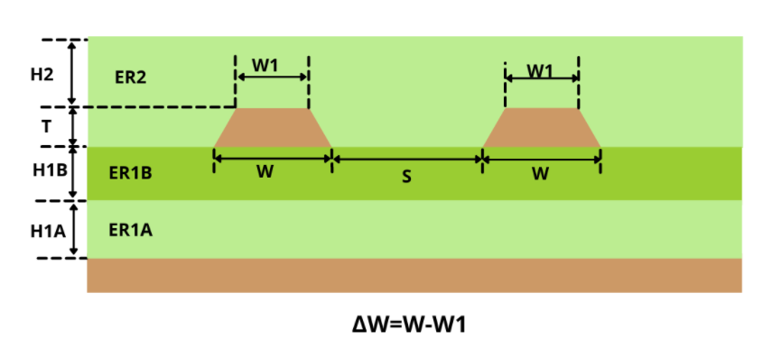
Differential signaling relies on balanced transmission lines where the differential impedance, typically targeted around 90 to 120 ohms depending on the protocol, defines signal propagation characteristics. This impedance arises from the interaction between the two traces and their reference planes, influenced by trace width, spacing, thickness, and dielectric constant. Variations in these parameters cause impedance discontinuities, resulting in reflections that distort waveforms. Maintaining symmetry ensures equal propagation delays and minimizes mode conversion from differential to common mode, which amplifies noise susceptibility.
Skew in differential pairs refers to length differences between the positive and negative traces, leading to phase misalignment at the receiver. Intra-pair skew directly impacts eye opening and jitter, while inter-pair skew affects multi-lane interfaces. Common-mode noise occurs when imbalances couple unwanted signals equally to both lines, potentially overwhelming the receiver's rejection capabilities. Reference planes provide return paths, and discontinuities like vias disrupt current distribution, exacerbating these effects.
Best Practices for Differential Pair Impedance Control
Achieving consistent differential pair impedance starts with stackup planning, where layer thicknesses and materials are selected to support target values. Engineers calculate trace geometry using field solvers, ensuring edge-coupled microstrip or stripline configurations maintain the specified impedance profile. Route pairs with constant spacing, typically 4 to 6 times the trace width for optimal coupling, and avoid abrupt changes that introduce mismatches. IPC-2221 outlines generic requirements for printed board design, emphasizing uniform trace parameters to preserve impedance integrity.
During routing, verify impedance at multiple points using post-layout simulations, adjusting for manufacturing tolerances like etch variation. Prefer outer layers for microstrip pairs to simplify fabrication, while inner striplines offer better shielding at the cost of tighter coupling control. Fabricators provide test coupons per IPC-2141 to validate impedance on production panels, confirming design margins. This systematic approach ensures high-speed signals propagate with minimal distortion.
Skew Control Techniques in Differential Pair Routing
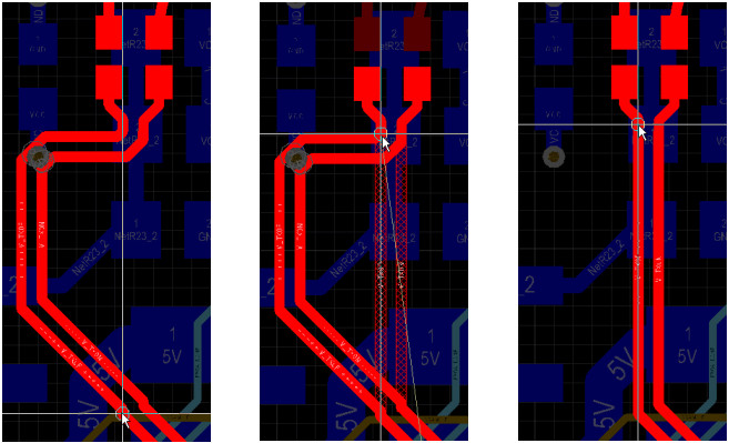
Skew control demands precise length matching within the pair, often to within a fraction of the signal rise time converted to distance. Use interactive length-tuning tools to serpentine the shorter trace, avoiding sharp bends that increase radiation. For multi-pair buses, align inter-pair lengths to prevent systematic skew across lanes. Route pairs as unbroken as possible, minimizing phase shifts from dielectric inconsistencies.
In practice, establish length tolerances early based on data rate; for example, tighter control for 25 Gbps signals. Simulate skew impacts on timing budgets, iterating layouts until margins are met. Maintaining symmetry in meanders preserves coupling and impedance simultaneously.
Maintaining Symmetry in Differential Pair Routing
Symmetry prevents mode conversion by ensuring identical environments for both traces, including bends, layer transitions, and proximity to other signals. Route pairs parallel with smooth 45-degree or curved corners to equalize path lengths and fields. Mirror routing patterns when crossing obstacles, avoiding one trace veering farther from the reference plane. Orthogonal routing to adjacent pairs reduces crosstalk while preserving balance.
Asymmetric etch or plating can introduce imbalances, so design with fab capabilities in mind. Post-route reviews check for deviations, with DRC rules enforcing symmetry constraints.
Minimizing Vias in Differential Pairs
Vias introduce parasitic inductance and capacitance, disrupting differential pair impedance and symmetry. Plan routing to avoid layer changes, dedicating signal layers adjacent to planes. When unavoidable, use via-in-pad or backdrilled vias to shorten stubs, placing them as coupled pairs with ground vias nearby for shielding. Limit via count per pair to one or two, optimizing fanout from BGA packages.
Tuned via structures with optimized antipads maintain impedance continuity. Simulate via effects early, as they contribute significantly to insertion loss at high frequencies.
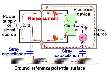
Strategies for Common Mode Noise Reduction
Common mode noise reduction hinges on balanced routing and solid reference planes under the pairs. Split planes require stitching vias to provide low-impedance returns, preventing ground bounce coupling. Increase spacing to single-ended signals and avoid running pairs near power traces. Shield pairs with grounded guard traces where density demands it.
IPC-6012 specifies performance criteria for rigid boards, including controlled impedance verification to support noise immunity. Comprehensive simulation validates rejection ratios before fabrication.
Troubleshooting Common Differential Pair Issues
Engineers often encounter eye closure from excessive skew or impedance mismatches during prototyping. Review S-parameters for reflections peaking at via frequencies, then adjust backdrilling. Crosstalk appears as correlated noise; widen inter-pair spacing or add shielding. Fabrication variations like uneven copper demand design margins and test coupons.
A structured debug flow involves TDR measurements, cross-section analysis, and redesign iterations. Case studies show that early symmetry enforcement resolves 80% of signal integrity failures.
Conclusion
Mastering differential pair routing requires integrating impedance control, skew management, symmetry, via minimization, and noise reduction into the design workflow. These practices ensure robust high-speed performance, aligning with industry standards for reliability. Electric engineers benefit from simulation-driven layouts and fab collaboration to hit targets consistently. Implementing these guidelines elevates PCB designs to meet demanding applications without costly respins.
FAQs
Q1: How do you control differential pair impedance during routing?
A1: Differential pair impedance control involves precise trace width, spacing, and stackup design per guidelines like IPC-2141. Verify with field solvers and post-layout extraction, targeting protocol specs. Manufacturing test coupons confirm production values, accounting for tolerances.
Q2: What is skew control in differential pairs and why is it critical?
A2: Skew control minimizes length differences within pairs to prevent timing errors in high-speed transmission. Use length-tuning for matching, simulating impacts on jitter. Proper control maintains eye diagram integrity for reliable data recovery.
Q3: Why focus on maintaining symmetry in differential pair routing?
A3: Maintaining symmetry avoids mode conversion and ensures balanced propagation delays. Route traces parallel with identical bends and environments. This practice supports common mode noise reduction and overall signal quality.
Q4: How can minimizing vias in differential pairs improve performance?
A4: Minimizing vias in differential pairs reduces discontinuities and preserves impedance profile. Coupled via placement with backdrilling mitigates stubs. Fewer transitions lower loss and simplify symmetry enforcement.
References
IPC-2141A — Design Guide for High-Speed Controlled Impedance Transmission Line Structures. IPC, 2017
IPC-2221B — Generic Standard on Printed Board Design. IPC, 2016
IPC-6012E — Qualification and Performance Specification for Rigid Printed Boards. IPC, 2017


