Introduction
Electromagnetic interference poses significant challenges in modern printed circuit board design, particularly as operating frequencies increase and component densities rise. PCB designers must prioritize EMI and EMC compliance to ensure reliable performance and regulatory approval. Effective PCB layout practices directly influence noise emission and noise generation, making them critical for high-speed electronics. This article explores fundamental principles, mechanisms, and strategies tailored for electric engineers. By understanding these elements, designers can mitigate risks early in the development cycle. Compliance not only avoids costly redesigns but also enhances product robustness in electromagnetic environments.
Electromagnetic interference, or EMI, refers to the disruption caused by electromagnetic radiation from one electronic device to another. Electromagnetic compatibility, or EMC, encompasses the ability of equipment to function correctly in its electromagnetic environment without causing or suffering unacceptable degradation. Emissions represent noise generation that radiates or conducts outward, while immunity addresses susceptibility to external interference. For PCB designers, PCB layout EMI and EMC compliance determines whether a board passes certification tests and operates reliably alongside other systems. Failure to address these can lead to intermittent failures, data corruption, or outright rejection by regulatory bodies. In dense electronic systems, poor layout amplifies noise emission, underscoring the need for proactive design strategies.
Regulatory frameworks demand strict limits on radiated and conducted emissions to prevent interference with communication systems and medical devices. PCB layout decisions, such as trace routing and plane allocation, form the foundation of compliance efforts. Engineers targeting high-speed signals face heightened risks due to faster edge rates that generate broadband noise. Integrating EMC considerations from schematic capture through layout verification saves time and resources. Ultimately, mastering these concepts elevates design quality and market readiness.
What Is EMI and EMC and Why It Matters for PCB Designers
Electromagnetic interference, or EMI, refers to the disruption caused by electromagnetic radiation from one electronic device to another. Electromagnetic compatibility, or EMC, encompasses the ability of equipment to function correctly in its electromagnetic environment without causing or suffering unacceptable degradation. Emissions represent noise generation that radiates or conducts outward, while immunity addresses susceptibility to external interference. For PCB designers, PCB layout EMI and EMC compliance determines whether a board passes certification tests and operates reliably alongside other systems. Failure to address these can lead to intermittent failures, data corruption, or outright rejection by regulatory bodies. In dense electronic systems, poor layout amplifies noise emission, underscoring the need for proactive design strategies.
Regulatory frameworks demand strict limits on radiated and conducted emissions to prevent interference with communication systems and medical devices. PCB layout decisions, such as trace routing and plane allocation, form the foundation of compliance efforts. Engineers targeting high-speed signals face heightened risks due to faster edge rates that generate broadband noise. Integrating EMC considerations from schematic capture through layout verification saves time and resources. Ultimately, mastering these concepts elevates design quality and market readiness.
Mechanisms of Noise Generation and Emission in PCBs
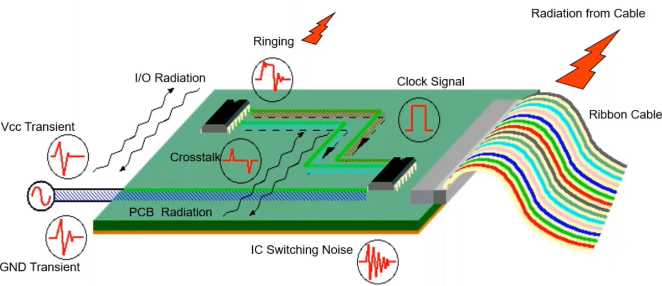
Noise generation in PCBs primarily stems from rapid switching transients in digital circuits, power converters, and clock oscillators. These events create high-frequency currents that propagate through traces and planes, forming unintended antennas. Radiated emissions occur when current loops enclose significant area, converting electrical energy into electromagnetic fields. Conducted emissions travel via power and ground lines, coupling into cables. PCB layout directly influences these paths, amplifying or suppressing noise based on geometry and materials.
Return currents seek the lowest impedance path, often spreading across planes if not controlled. High di/dt in switching nodes induces voltage spikes via parasitic inductances, exacerbating noise emission. Clock harmonics extend into GHz ranges, where PCB structures resonate efficiently. Understanding these mechanisms allows designers to target root causes rather than symptoms. For instance, long parallel traces act as coupled lines, injecting crosstalk that contributes to overall noise generation.
Susceptibility arises when external fields induce voltages in sensitive loops, flipping logic states or corrupting analog signals. Ground bounce from simultaneous switching further generates noise that radiates from IC packages. These interactions highlight the bidirectional nature of EMI in PCB environments.
Key PCB Layout Techniques for EMI and EMC Compliance
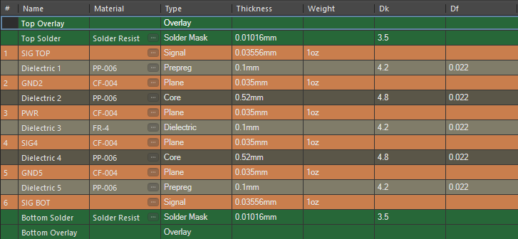
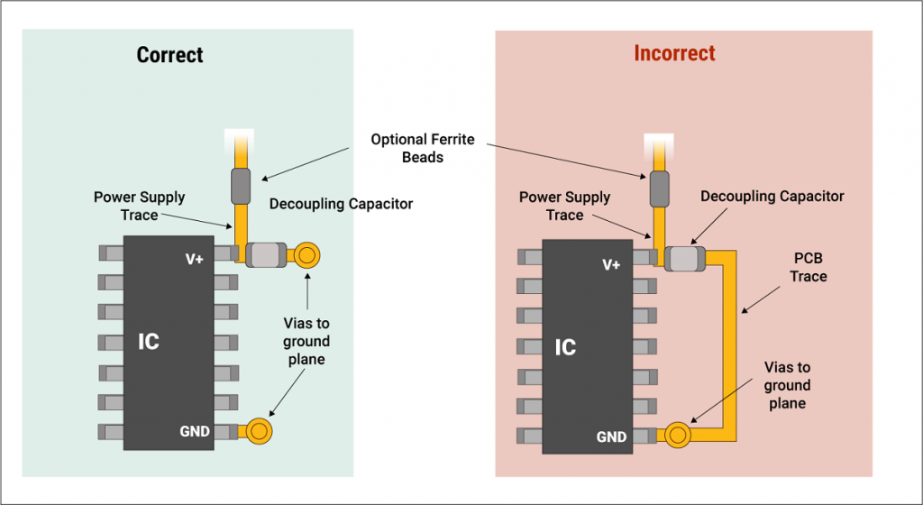
A well-planned layer stackup forms the cornerstone of PCB layout EMI and EMC optimization. Multilayer boards should dedicate inner layers to continuous ground and power planes, sandwiching signal layers between them for tight field confinement. This configuration minimizes loop inductance and provides low-impedance return paths. Avoid splitting planes under high-speed signals to prevent current detours that enlarge loop areas. IPC-2221A outlines general guidelines for such arrangements to support signal integrity and EMC.Component placement strategy separates noisy elements like switching regulators from sensitive analog sections. Position high-current components near board edges with direct paths to planes, reducing trace lengths. Decoupling capacitors must reside within millimeters of power pins to shunt high-frequency noise locally. Proper sequencing ensures critical signals route first, avoiding congestion. These steps curb noise generation at its source.
Trace routing demands orthogonal patterns to minimize coupling between adjacent lines. Keep high-speed traces short and above solid reference planes, treating them as controlled-impedance microstrips or striplines. Guard traces or ground stitching vias along edges shield sensitive nets. Minimize vias on return paths to preserve low inductance. IPC-2251 provides insights into high-speed packaging that align with these practices for EMI control.
Grounding schemes evolve with frequency: single-point for low frequencies, multi-point via planes for RF. Stitch split planes with dense via arrays to equalize potentials and block slot antennas. Power plane cutouts should align with component footprints, avoiding overlaps that foster resonances. Ferrite beads and common-mode chokes on I/O lines filter conducted emissions effectively.
Filtering complements layout by placing pi-networks near connectors. Spread-spectrum clocking reduces peak spectral energy, easing radiated limits. Simulation tools verify pre-layout assumptions, but physical principles guide initial decisions.
Advanced Best Practices and Standards Integration
Adhering to established standards ensures repeatable success in PCB layout EMI and EMC. IEC 61000 series defines testing protocols for emissions and immunity, guiding design targets for various environments. Designers reference these alongside IPC documents to balance performance and compliance. Layer symmetry in stackups aids manufacturability while supporting EMC goals.
Partitioning divides the board into zones with dedicated grounds tied at a single point. This star grounding prevents noise circulation between sections. For mixed-signal boards, optoisolators or transformers maintain isolation. Thermal vias under power devices dissipate heat without compromising planes.
Shielding enclosures integrate with PCB design via grounded seams and filtered feedthroughs. However, layout alone achieves substantial reductions, often 20-30 dB in emissions through iterative refinement.
Troubleshooting Common EMI Issues in PCB Layouts
Excessive clock radiation often traces to long traces without ground referencing. Shorten paths or add series resistors to dampen edges. Ground bounce manifests as periodic jitter; add more decoupling and check plane integrity. Conducted noise on power lines responds to LC filters sized for dominant frequencies.
Radiated peaks at board resonances require modal analysis or ferrite clamps. Crosstalk spikes indicate parallel routing; reroute perpendicularly. Pre-compliance testing with spectrum analyzers pinpoints culprits early. Systematic verification against standards prevents field returns.
Conclusion
PCB layout EMI and EMC compliance hinges on disciplined application of principles like solid planes, minimal loops, and strategic placement. Addressing noise emission and noise generation through these methods yields compliant, reliable boards. Electric engineers benefit from structuring designs around proven mechanisms and standards. Early integration avoids late-stage headaches and elevates product quality. Continuous learning and testing refine expertise in this evolving field.
FAQs
Q1: How does PCB layout impact EMI and EMC compliance?
A1: PCB layout EMI and EMC directly controls noise emission by defining current paths and antenna structures. Solid ground planes and tight loop areas reduce radiated fields, while proper decoupling shunts conducted noise. Strategic routing prevents coupling, ensuring immunity to external interference. Compliance hinges on these choices from stackup to final routing.
Q2: What are primary sources of noise generation in PCB designs?
A2: Noise generation arises from switching transients, clocks, and power supplies creating high di/dt currents. These propagate via traces, forming loops that emit broadband energy. Parasitic inductances amplify spikes, coupling into nearby nets. Layout mitigation like plane referencing contains these effects effectively.
Q3: Why prioritize ground planes in PCB layout for EMI reduction?
A3: Ground planes provide low-impedance returns, minimizing loop areas and inductance for noise emission control. They shield layers and distribute currents evenly, curbing resonances. Continuous pours avoid slots that radiate. This foundational practice aligns with standards for robust EMC performance.
Q4: Can PCB layout alone achieve EMC compliance?
A4: PCB layout significantly reduces noise generation and emissions, often meeting limits without extras. Techniques like orthogonal routing and decoupling handle most issues. However, combine with filtering for edge cases. Testing validates the approach iteratively.
References
IPC-2251 — Design Guide for the Packaging of High Speed Electronics Circuits. IPC, 2003
IPC-2221A — Generic Standard on Printed Board Design. IPC, 2003
IEC 61000-6-1 — Electromagnetic compatibility (EMC) - Part 6-1: Generic standards - Immunity for residential, commercial and light-industrial environments. IEC, 2016


