Introduction
Ball Grid Array (BGA) packages are a cornerstone of modern electronics, enabling high-density connections in compact designs for applications ranging from consumer devices to industrial systems. However, connecting BGA packages to the rest of the printed circuit board (PCB) poses significant challenges in routing and fanout strategies. Proper design of vias, pads, and conductors is critical to ensure signal integrity, thermal management, and manufacturability. This article explores the intricacies of BGA fanout and PCB routing, focusing on via types, pad design, and conductor routing best practices. Aimed at electrical engineers, the content provides structured guidance to optimize layouts for reliability and performance while adhering to recognized industry standards. Let’s dive into the technical details of connecting BGA packages effectively.
What Are BGA Packages and Why Do They Matter
BGA packages are surface-mount components with an array of solder balls on the underside, replacing traditional pins for connections. This design allows for a higher number of interconnects in a smaller footprint, making them ideal for complex integrated circuits like microprocessors and field-programmable gate arrays. The importance of BGA packages lies in their ability to support high-speed signals and dense layouts, which are essential in modern electronics. However, their dense pin arrangements create unique challenges in PCB routing, requiring precise fanout techniques to break out signals to other board layers. Without proper planning, issues like signal crosstalk, impedance mismatches, and manufacturing defects can arise. Understanding how to manage these connections is vital for ensuring functionality and reliability in high-performance designs.
Technical Principles of BGA Fanout and Routing
Understanding Fanout in BGA Packages
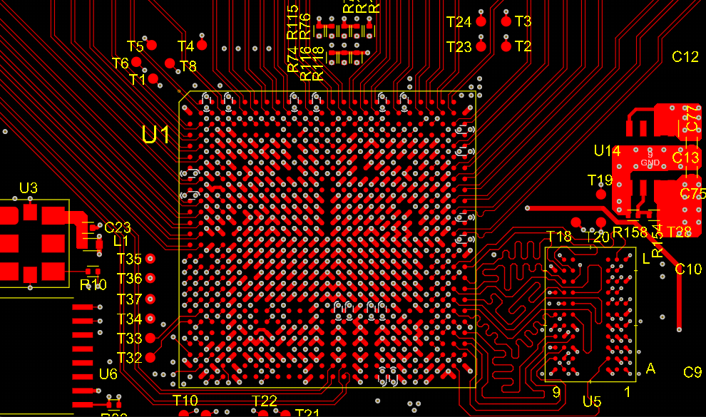
Fanout refers to the process of routing signals from the dense grid of BGA solder balls to the wider spacing of the PCB’s internal or external layers. The primary goal is to escape the tight pitch of BGA packages, often ranging from 0.5 mm to 1.27 mm, to areas where traces can be routed more freely. There are two main fanout strategies: dog-bone and via-in-pad. The dog-bone approach uses a short trace connecting the BGA pad to a nearby via, allowing signals to transition to other layers. Via-in-pad, conversely, places the via directly under the BGA pad, saving space but requiring advanced manufacturing techniques to prevent solder wicking.
Role of Via Types in Routing
Via types play a crucial role in BGA routing. Through-hole vias, extending through all layers, are simple but consume valuable space in multilayer boards. Blind vias connect an outer layer to an inner layer without passing through the entire board, offering flexibility for dense designs. Buried vias link internal layers only, further optimizing space. The choice of via type impacts signal integrity, especially for high-speed signals where minimizing inductance and capacitance is essential. Standards like IPC-2221B provide guidelines on via placement and sizing to balance electrical performance with manufacturing constraints.
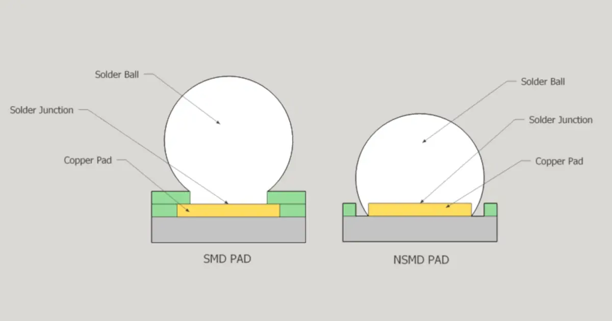
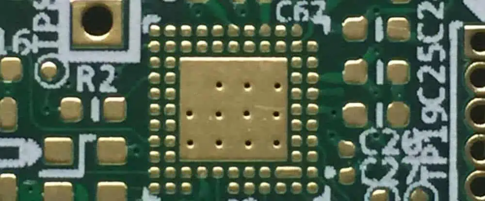
Pad Design Considerations
Pad design for BGA packages must ensure reliable soldering and alignment during assembly. Non-solder mask defined (NSMD) pads, where the solder mask opening is larger than the pad, are often preferred for BGA packages. NSMD pads allow better solder joint formation and reduce stress on the connection, as outlined in IPC-7351B. The pad size and shape must match the solder ball dimensions to prevent defects like bridging or insufficient wetting. Additionally, thermal pads under BGA packages may require specific patterns to manage heat dissipation effectively.
Conductor Routing Challenges
Conductor routing for BGA packages involves navigating a high-density grid while maintaining signal integrity. Traces must avoid sharp bends to minimize reflections, especially for high-speed signals. Differential pairs, common in BGA designs, require matched lengths and consistent spacing to prevent skew. Crosstalk can be mitigated by maintaining adequate separation between traces or using ground planes as shields. Adhering to impedance control guidelines, as specified in IPC-2141A, ensures consistent signal transmission across the board.
Best Practices for BGA Fanout and PCB Routing
Planning the Fanout Strategy
Effective fanout begins with careful planning of via placement and layer assignment. For smaller BGA packages, a simple dog-bone fanout on the top layer may suffice, routing signals to adjacent vias. Larger packages with hundreds of pins often require a mix of blind and buried vias to access multiple layers without congestion. Prioritize power and ground pins for direct connections to planes, reducing noise and improving stability. Simulation tools can help visualize signal paths and identify potential bottlenecks before finalizing the layout.
Optimizing Via Types for Density and Performance
Selecting the right via type is essential for balancing density and performance. Blind vias are useful for connecting BGA signals to inner signal layers without occupying space on lower layers. Buried vias can link internal power or ground planes, freeing up surface area for critical traces. Ensure via diameters and annular rings comply with IPC-6012E to avoid manufacturing issues. For high-speed designs, minimize via stubs, as they can introduce unwanted signal reflections.
Pad Design for Reliability
When designing pads for BGA packages, follow industry standards like IPC-7351B for sizing and spacing. Use NSMD pads to enhance solder joint reliability, especially for fine-pitch components. Ensure the solder mask opening provides sufficient clearance to avoid masking errors during fabrication. For thermal management, incorporate a grid of microvias or thermal vias under central pads to dissipate heat to a ground plane, following guidelines in IPC-2222A.
Conductor Routing Guidelines
Route high-speed signals first to secure optimal paths, avoiding crossovers and maintaining consistent trace widths for impedance control. Use 45-degree angles for trace bends to reduce signal reflections. For differential pairs, keep traces parallel and equidistant from ground planes to maintain symmetry. Ground planes should be continuous under BGA packages to provide a low-impedance return path, as recommended by IPC-2221B. Avoid routing traces directly under BGA pads unless necessary, to minimize interference.
Layer Stackup and Power Distribution
A well-designed layer stackup is critical for BGA routing. Allocate dedicated layers for power and ground planes near the BGA to minimize loop inductance. Place signal layers adjacent to ground planes to control impedance and reduce electromagnetic interference. For the multilayer circuit board, a typical stackup might include top and bottom signal layers, with inner layers for power and ground. Follow IPC-2222A for layer spacing and dielectric thickness to ensure manufacturability and electrical performance.
Troubleshooting Common BGA Routing Issues
BGA routing often encounters challenges like signal crosstalk, incomplete fanout, or manufacturing defects. Crosstalk can occur when traces are too close, especially in dense areas near the BGA. Adding ground vias or increasing trace spacing can mitigate this issue. Incomplete fanout, where some pins remain unconnected, may result from poor via placement. Revisiting the fanout strategy or using additional layers can resolve this. Manufacturing defects, such as misaligned vias, often stem from inadequate design rules. Adhering to IPC-6012E ensures vias and pads meet fabrication tolerances. For high-speed designs, signal integrity analysis during the design phase can preempt issues like impedance mismatch or excessive noise.
Conclusion
Connecting BGA packages to the rest of the fast turn PCB through effective fanout and routing is a complex but essential task for electrical engineers. By understanding the principles of via types, pad design, and conductor routing, designers can create layouts that ensure signal integrity and reliability. Best practices, such as strategic via placement, optimized pad configurations, and careful trace routing, form the foundation of successful BGA integration. Following industry standards like those from IPC ensures manufacturability and performance in high-density designs. With meticulous planning and attention to detail, engineers can overcome the challenges of BGA packages and achieve robust PCB layouts for modern electronics.
FAQs
Q1: What are the main challenges in PCB routing for BGA packages?
A1: Routing BGA packages is challenging due to their high pin density and tight pitch, often requiring complex fanout strategies. Signal integrity issues like crosstalk and impedance mismatch can arise without proper planning. Additionally, balancing thermal management and manufacturability adds complexity. Following standards like IPC-2221B helps address these issues by providing guidelines for via placement and trace spacing to ensure reliable connections.
Q2: How do via types impact BGA fanout design?
A2: Via types significantly affect BGA fanout by determining how signals transition between layers. Through-hole vias are simple but space-intensive, while blind vias save space by connecting only to specific layers. Buried vias optimize internal routing. Choosing the right type, as per IPC-6012E, balances density and performance, ensuring minimal signal loss and manufacturability in dense BGA layouts.
Q3: Why is pad design critical for BGA packages on PCBs?
A3: Pad design is vital for BGA packages to ensure reliable solder joints and alignment during assembly. Non-solder mask defined pads, recommended by IPC-7351B, improve joint strength by allowing better solder flow. Proper sizing prevents defects like bridging. Well-designed pads also aid thermal dissipation, critical for maintaining component performance under operational stress.
Q4: What are best practices for conductor routing in BGA designs?
A4: For conductor routing in BGA designs, prioritize high-speed signals to secure optimal paths. Maintain consistent trace widths for impedance control per IPC-2141A. Use 45-degree bends to minimize reflections and ensure differential pairs are symmetrical. Incorporate ground planes for noise reduction. These practices help achieve reliable signal transmission in dense BGA layouts.
References
IPC-2221B — Generic Standard on Printed Board Design. IPC, 2012.
IPC-2222A — Sectional Design Standard for Rigid Organic Printed Boards. IPC, 2010.
IPC-6012E — Qualification and Performance Specification for Rigid Printed Boards. IPC, 2020.
IPC-7351B — Generic Requirements for Surface Mount Design and Land Pattern Standard. IPC, 2010.
IPC-2141A — Design Guide for High-Speed Controlled Impedance Circuit Boards. IPC, 2004.


