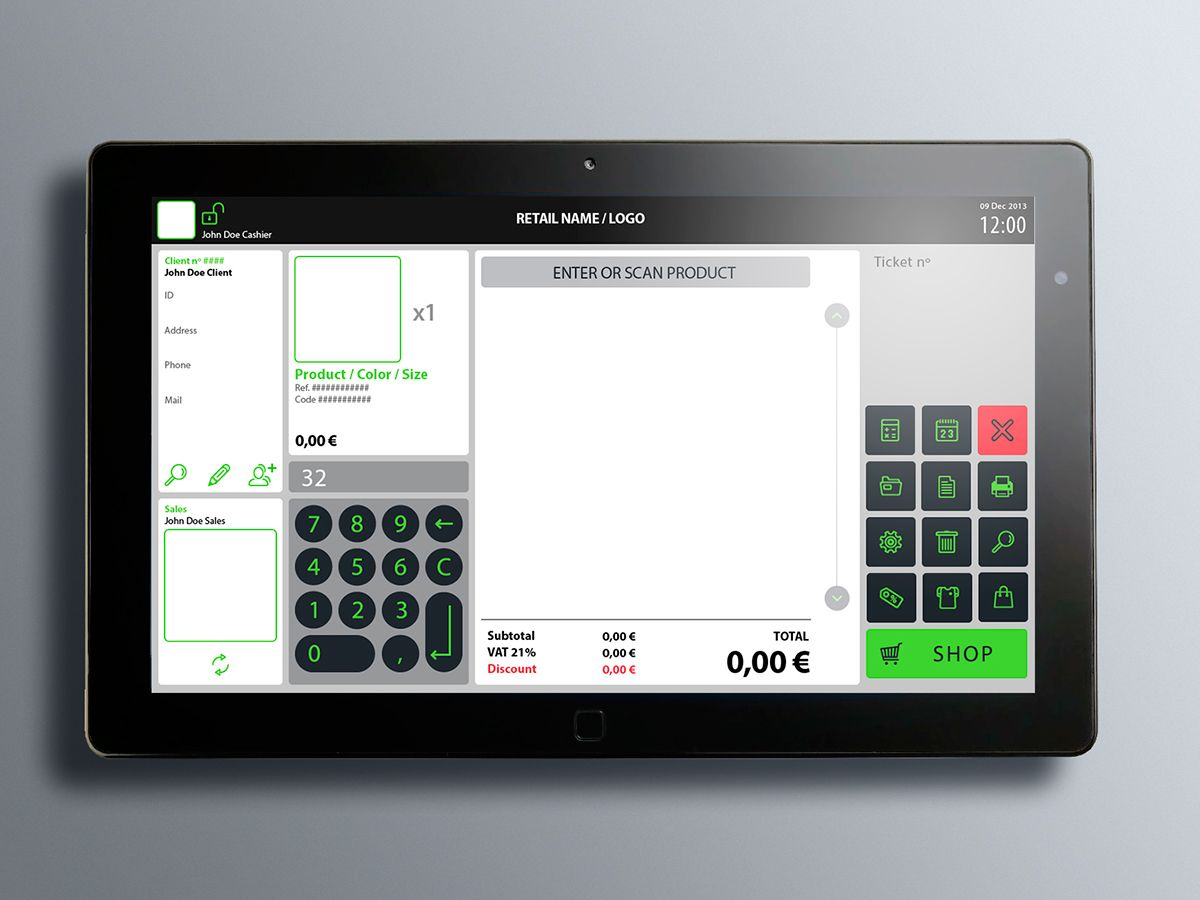
Why is PCB Security Crucial for Point-of-Sale Systems?
Point-of-Sale (POS) systems serve as the core infrastructure for retail transactions, processing millions of payments daily. However, their involvement in handling sensitive financial data makes them attractive targets for various attacks, including skimming, data theft, and physical tampering. A security breach in a POS system can lead to substantial financial losses, reputational damage, and severe legal repercussions. This is precisely where a thoughtful POS PCB security design becomes indispensable. A meticulously engineered printed circuit board (PCB) acts as the primary defense mechanism, safeguarding the hardware from unauthorized access and ensuring adherence to critical standards like PCI DSS (Payment Card Industry Data Security Standard).
Prioritizing security during the PCB design phase can prevent costly revisions and mitigate vulnerabilities later in the product lifecycle. Let's delve into the fundamental aspects of creating a tamper-proof POS system, beginning with the core principles of security-focused PCB development.
What Are the Foundational Principles of Secure POS PCB Design?
Crafting a secure PCB for a POS system demands a comprehensive, multi-layered strategy that addresses both physical and digital threats. Adhering to these core principles will guide your design process:
Adopting a Layered Security Framework
Security is not a singular feature but rather a synergistic combination of multiple defensive mechanisms. A layered approach integrates physical barriers, encrypted data pathways, and sophisticated tamper-detection systems. For instance, incorporating a secure microcontroller equipped with hardware-based encryption ensures that even if one security layer is compromised, others remain intact. This significantly reduces the risk of a single point of failure in the system.
Ensuring Compliance with PCI DSS Standards
PCI DSS represents a stringent set of security standards specifically created to safeguard cardholder data. A PCB design that is PCI DSS compliant must integrate features such as encrypted communication channels and secure storage solutions for sensitive information. Non-compliance can lead to substantial fines or the revocation of certification, making it imperative to factor these standards into the design process from the outset.
Addressing Both Physical and Digital Threats
POS systems face a dual threat landscape: physical tampering (e.g., attempts to drill into the device to access internal components) and digital attacks (e.g., intercepting data signals). Your PCB design should proactively address both categories by incorporating robust anti-tampering PCB features alongside secure data transmission protocols.
What Anti-Tampering Features Should Be Integrated into POS PCBs?
Physical tampering represents a frequent attack vector for POS systems, where malicious actors might attempt to gain access to internal components to extract data or install illicit hardware. Integrating anti-tampering PCB features can effectively deter or detect such attempts. Here are some proven strategies:
Tamper-Detection Mechanisms
Embed sensors designed to identify unauthorized access, such as pressure or motion sensors. For example, a fine mesh layer within the PCB can trigger an alarm or initiate the wiping of sensitive data if an attempt is made to drill through the board. These sensors should be connected to a secure microcontroller capable of logging or responding to any detected tampering incidents.
Protective Barriers and Concealment
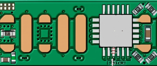
Apply epoxy coatings or potting compounds over critical components to significantly complicate reverse engineering efforts. These materials solidify around the PCB, creating a robust physical barrier. Furthermore, design the PCB to be housed within a tamper-resistant enclosure, utilizing specialized screws or seals that visibly indicate any attempt at disturbance. Conceal critical signal paths by designing the PCB with buried traces and blind vias. By routing sensitive data lines on internal layers of a multilayer PCB (e.g., a 6-layer or 8-layer board), it becomes considerably more difficult for attackers to probe or intercept signals. Ensure that the impedance for these traces is carefully controlled, typically around 50 ohms for high-speed signals, to preserve signal integrity.
How is a Secure Microcontroller Integrated in POS PCB Design?
The microcontroller functions as the central processing unit of a POS system, managing data processing and communication. Integrating a secure microcontroller is vital for protecting against firmware attacks and unauthorized access. Here’s how to implement it effectively:
Selecting a Microcontroller with Intrinsic Security
Opt for a microcontroller that features hardware-based security capabilities, such as secure boot functionality, encrypted memory, and integrated tamper detection. These features are essential for ensuring that firmware cannot be altered without proper authorization and that sensitive data is stored in a protected manner.
Isolating Critical Functions and Secure Updates
Design the PCB to physically isolate the microcontroller from other components by utilizing dedicated power and ground planes. This measure reduces the likelihood of electromagnetic interference (EMI) and mitigates side-channel attacks, where adversaries might analyze power consumption patterns to extract data. For instance, maintain a minimum separation of 0.5 mm between sensitive traces and other signals to minimize crosstalk. Furthermore, mandate that firmware updates occur exclusively through encrypted channels. Design the PCB to support a secure bootloader that rigorously verifies the authenticity of updates using digital signatures before they are installed. This prevents the introduction of malicious code into the system.
What Are the Best Practices for Encryption Module PCB Layout?
Encryption is a foundational element of POS security, ensuring that sensitive data, such as cardholder information, remains impenetrable to unauthorized individuals. A meticulously designed encryption module PCB layout is paramount for achieving effective data protection. Adhere to these best practices:
Dedicated Hardware and Signal Protection
Utilize a specialized encryption module or chip to manage data encryption and decryption processes. This approach not only offloads processing demands from the main microcontroller but also enhances security by isolating cryptographic functions. Ensure that the chosen module supports robust algorithms like AES-256, which is widely recognized for securing payment data. Route encryption-related traces on internal layers of the PCB to minimize the risk of signal interception. Keep trace lengths as short as possible—ideally under 10 mm for high-speed signals—to reduce electromagnetic radiation that could potentially be captured by attackers. Employ differential signaling for critical data pathways to further diminish noise and interference.
Secure Key Management
Design the PCB to incorporate secure storage for encryption keys, such as a hardware security module (HSM). Avoid storing keys in easily accessible memory locations. Physically separate the key storage area from other components, and utilize shielding to protect against electromagnetic attacks that could attempt to extract these keys.
How Does PCI DSS Compliance Shape PCB Design?
Adherence to PCI DSS is an absolute requirement for POS systems. A PCB design that is PCI DSS compliant ensures that your hardware meets the rigorous security mandates for handling payment data. Here are crucial considerations:
Secure Data Pathways and Physical Safeguards
Design the HDI PCB to support point-to-point encryption (P2PE), which encrypts data from the moment it is entered until it reaches the payment processor. This significantly reduces the window of vulnerability for data theft. Ensure that communication interfaces, such as USB or Ethernet, are secured with appropriate shielding and filtering to prevent data leakage. PCI DSS mandates physical protection against tampering. Incorporate tamper-evident designs, such as seals or labels that visibly break if the device is opened. Additionally, ensure that all connectors and ports are either secured or disabled when not in use to prevent unauthorized access.
Facilitating Security Audits
While not a direct design element, PCB layouts should be conducive to testing for vulnerabilities. Include test points for security audits, but ensure these are either protected or completely disabled in production units to prevent their exploitation. Collaborate with independent third-party assessors to verify compliance during the design and development phases.
H2: What Additional Measures Enhance Tamper-Proof POS PCB Design?
Beyond the core components, several additional strategies can significantly bolster the security of your POS PCB design:
Power Management and Thermal Stability
Implement tamper-resistant power circuits to prevent attackers from disabling security features by cutting power. Incorporate backup power sources, such as capacitors, to sustain critical functions during an attempted attack. Ensure effective heat dissipation for secure components. Overheating can degrade the performance of encryption modules or microcontrollers, so utilize heat sinks or thermal vias to maintain operating temperatures below 85°C.
Controlled Documentation
Strictly control access to PCB design files and schematics. Limit access to only authorized personnel and employ encrypted file storage to prevent the theft of valuable intellectual property.
Navigating Challenges in Secure POS PCB Design
Engineers often face challenges when implementing these best practices, such as balancing stringent security requirements with cost constraints, managing limited board space for additional features, and staying abreast of ever-evolving security threats. To address these, prioritize critical security features based on comprehensive risk assessments, and opt for modular designs that facilitate future upgrades without necessitating a complete overhaul.
For example, a compact POS system may have insufficient space for multiple tamper-detection sensors. In such scenarios, consider integrated solutions that combine several security features into a single chip or module, minimizing the physical footprint while maintaining robust protection.
Conclusion: Building Trust Through Advanced PCB Security
The foundation of a tamper-proof POS system begins with a security-first approach at the PCB level. By concentrating on robust POS PCB security design, incorporating advanced anti-tampering features, ensuring seamless secure microcontroller integration, optimizing encryption module PCB layouts, and adhering strictly to PCI DSS compliant PCB design principles, you can develop resilient systems that safeguard transactions and cultivate customer trust.
At AIVON, we deeply understand the critical importance of secure hardware in today's digital landscape. Our extensive expertise in PCB manufacturing and assembly can transform your secure POS designs into reality with unparalleled precision and reliability. By adopting the best practices outlined in this guide, you are taking a crucial step toward protecting sensitive data and ensuring compliance with industry benchmarks. Let's collaborate to secure every transaction, one meticulously designed PCB at a time.


