Introduction
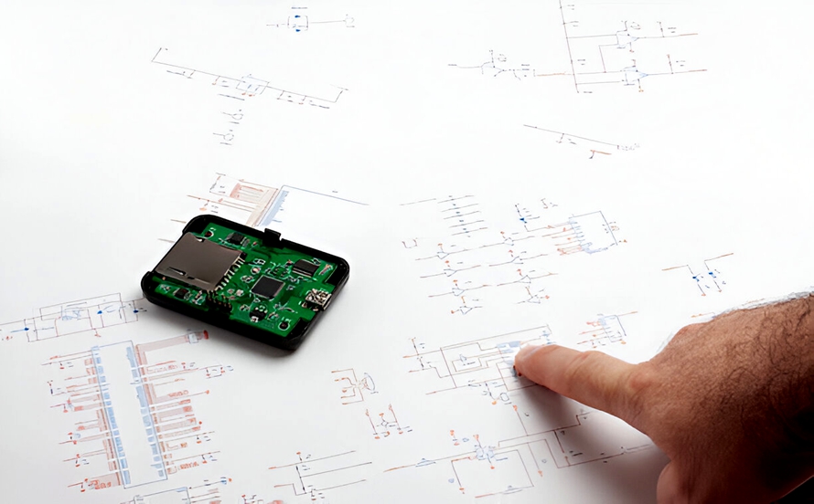
Every innovative electronic project often begins with a simple sketch on a napkin, capturing the essence of a circuit idea in rough lines and notes. For electronic hobbyists, transforming this initial concept into a professional PCB schematic marks the exciting entry into actual hardware realization. This easy PCB schematic tutorial will guide you through the process, from capturing your idea digitally to generating Gerber files ready for fabrication. Understanding schematic design empowers hobbyists to create reliable simple PCB project schematics without overwhelming complexity. By following structured steps, you avoid common pitfalls and build confidence in handling beginner PCB design software. Ultimately, this journey bridges creativity with practical engineering, enabling you to prototype custom boards for your projects.
What Is PCB Schematic Design and Why It Matters for Hobbyists
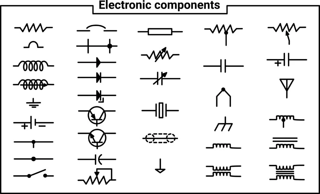
A PCB schematic serves as the blueprint of your electronic circuit, illustrating how components connect through symbols, nets, and annotations. Unlike a physical layout, it focuses on electrical functionality rather than physical placement, making it the foundational step before PCB layout. For hobbyists, mastering schematic design ensures signal integrity and prevents errors that could lead to faulty prototypes. It allows simulation of circuit behavior early, saving time and materials during testing. Industry relevance stems from its role in standardizing communication between designers and manufacturers, adhering to principles that promote reliability. In essence, a well-crafted schematic translates your napkin idea into a verifiable design ready for the next phases.
Schematics use standardized symbols for resistors, capacitors, integrated circuits, and other components to maintain clarity across tools and teams. Nets represent electrical connections, labeled to avoid ambiguity in complex designs. Power and ground planes are denoted distinctly to highlight distribution paths. Hobbyists benefit from this logical structure, as it facilitates troubleshooting and modifications. Without a solid schematic, transitioning to layout becomes chaotic, increasing the risk of shorts or open circuits.
Key Principles of Schematic Design
Effective schematic design relies on logical organization, starting with power input and flowing through signal paths to outputs. Components must be grouped by function, such as analog sections separate from digital to minimize noise coupling. Annotation includes reference designators, values, and tolerances for each part, ensuring completeness. Hierarchical sheets help manage larger projects by breaking them into modules. Following these principles aligns with engineering best practices, making your design scalable. For beginners, this structured approach turns abstract ideas into tangible diagrams.
Net naming conventions enhance readability, using descriptive labels like VCC_5V or GND instead of generic terms. Buses group multiple related signals, reducing clutter in dense schematics. Junction dots clearly indicate connections, while no-connect flags prevent unintended links. These elements ensure the schematic accurately reflects circuit intent. Hobbyists often overlook annotations initially, but they prove crucial during assembly and debugging.
Choosing Features in Beginner PCB Design Software
Beginner PCB design software should offer intuitive schematic capture with drag-and-drop symbols and auto-routing previews. Look for libraries with common through-hole and surface-mount components, plus easy net labeling tools. Simulation integration allows verifying logic before layout, a key feature for hobbyists iterating designs. User-friendly interfaces with zoom, pan, and undo support speed up the learning curve. Cross-platform compatibility ensures accessibility on various devices. Prioritize software with built-in design rule checks to flag errors early.
Integrated schematic-to-layout forward annotation automates component placement and netlist generation. Custom symbol editors let you create parts for unique needs. Bill of materials export simplifies procurement. These features make the transition smooth for simple projects. Hobbyists appreciate tutorials and community resources within the software ecosystem.
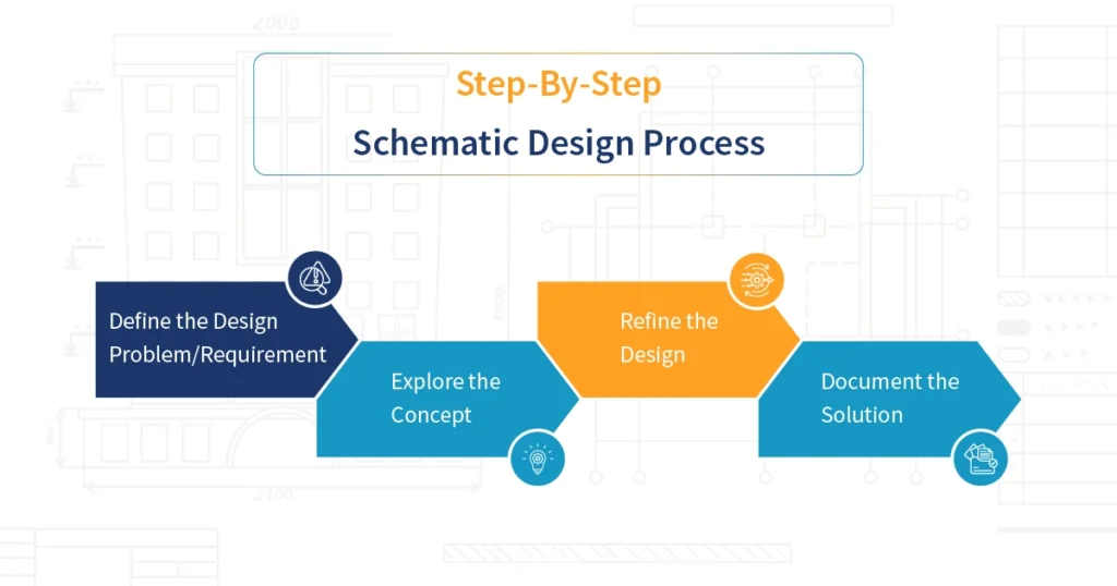
Step-by-Step Easy PCB Schematic Tutorial
Start by opening a new schematic in your beginner PCB design software and setting the sheet size to A4 or letter for manageability. Place power symbols first, connecting to a ground plane reference. Add components from the library, assigning reference designators sequentially like R1, C1. Draw wires for nets, labeling multi-point connections. Annotate values and add text notes for clarity. Compile the design to check for errors like floating pins.
Next, organize components into functional blocks using rectangles or hierarchical pins. Simulate the circuit if available, adjusting for issues like incorrect polarities. Generate a netlist, which lists all connections for layout import. Print or export the schematic for review. This process embodies a simple PCB project schematic workflow. Repeat refinements until the design functions as intended.
Transitioning to PCB Layout: A Hobbyist PCB Layout Guide
Once the schematic is complete, import the netlist into the PCB editor to place components on a board outline. Begin with critical parts like connectors and crystals near edges for mechanical stability. Space components to allow routing traces without excessive vias. Follow design rules for trace widths based on current needs, wider for power lines. Place decoupling capacitors close to IC power pins to reduce noise. This hobbyist PCB layout guide emphasizes iterative placement for optimal performance.
Route traces logically, prioritizing high-speed signals on inner layers if multilayer. Use ground pours to shield sensitive areas. Autorouters assist beginners, but manual tweaks ensure quality. Add silkscreen for labels and fiducials for alignment. Design rule checks verify spacing and clearances. Adhering to IPC-2221 guidelines here prevents issues like insufficient creepage distances in high-voltage sections.
Creating Gerber Files from Schematic Path
Gerber files translate your layout into manufacturing data, including copper layers, solder mask, and drill files. After finalizing the layout, select all layers and generate RS-274X format outputs. Include top/bottom copper, solder mask, silkscreen, and paste if assembling. Export Excellon drill files for holes. Verify files in a free viewer for completeness. Creating Gerber files from schematic via layout ensures fabricators receive accurate instructions.
Panelize boards for cost efficiency in small runs. Specify stackup details like layer count and thicknesses in fabrication notes. Job files consolidate outputs for easy submission. Hobbyists often generate these for prototypes, iterating based on assembly feedback. This step completes the napkin-to-production pipeline.
Best Practices and Industry Standards
Maintain consistent symbol orientations and pin numbering for intuitive reading. Use buses for parallel data lines to simplify diagrams. Implement power distribution networks with decoupling throughout. Check for unconnected pins and duplicate references during compilation. These practices reduce errors downstream. Following IPC-7351 for land pattern geometries ensures reliable soldering in assembly.
Document design decisions in notes, aiding future revisions. Simulate thermal effects for power components. Version control schematics to track changes. Standards like IPC-2221 provide frameworks for trace spacing and material selection, vital for hobbyist reliability. Avoid overcrowding to facilitate probing during debug.
A Simple LED Blinker Project Example
Consider a basic astable multivibrator using two transistors, resistors, and capacitors to blink an LED. Sketch the cross-coupled circuit on paper first. Digitize into schematic with timed components for 1Hz rate. Simulate to confirm oscillation. Forward to layout on a single-sided board under 50mm square. Generate Gerbers and fabricate for under $10.
This simple PCB project schematic teaches timing, biasing, and output drive. Troubleshoot by measuring voltages against expected values. Scale by adding a potentiometer for adjustable speed. Such projects build skills progressively.
Conclusion
Transforming a napkin sketch into Gerber files involves methodical schematic design, layout, and output generation. Key steps include symbol placement, net routing, rule checks, and verification. Hobbyist benefits include cost savings and custom functionality. Adhering to structured workflows and standards like IPC-2221 elevates prototypes to professional quality. Experiment with simple circuits to gain proficiency. Your ideas now have a clear path to reality.
FAQs
Q1: What is the easiest way to start an easy PCB schematic tutorial for beginners?
A1: Begin with a blank sheet in beginner PCB design software, place power symbols first, then add components from libraries. Connect nets logically and annotate values. Simulate if possible to verify function. Compile for errors before layout. This structured approach suits hobbyists building their first simple PCB project schematic.
Q2: How does a hobbyist PCB layout guide differ from schematic design?
A2: Schematic focuses on electrical connections via symbols, while layout arranges physical components and routes traces. Import netlist from schematic to preserve connectivity. Prioritize placement for signal integrity and manufacturability. Follow spacing rules per IPC-2221. The guide emphasizes iterative refinement for compact boards.
Q3: What steps are involved in creating Gerber files from schematic?
A3: Complete schematic, generate netlist, import to layout editor. Place components, route traces, add silkscreen. Select layers and export RS-274X Gerbers plus drills. View files to confirm. Include notes on stackup. This process prepares files for fabrication directly from your design.
Q4: Can beginners handle Gerber files without advanced software?
A4: Yes, beginner PCB design software includes built-in Gerber generators. After layout, one-click export creates all needed files. Verify with viewers for overlaps or misses. Start with single-layer for simplicity. Hobbyists successfully prototype this way repeatedly.
References
IPC-2221B — Generic Standard on Printed Board Design. IPC, 2009
IPC-7351B — Generic Requirements for Surface Mount Design and Land Pattern Standard. IPC, 2010
IPC-6012E — Qualification and Performance Specification for Rigid Printed Boards. IPC, 2017


