Transitioning from a schematic to a functional 8-layer PCB demands precision, especially in today's high-density electronics landscape. As a PCB design expert with over a decade optimizing layouts for telecommunications and automotive systems, I've guided countless teams through this process. An 8-layer board strikes a balance between complexity and performance, enabling high-speed signals up to 10 Gbps while managing EMI and thermal loads. Yet, poor layout choices—like unbalanced stackups or haphazard routing—can introduce crosstalk exceeding 10% or impedance mismatches beyond ±5%, derailing prototypes.
This guide demystifies 8-layer PCB layout best practices, walking you step-by-step from stackup planning to validation. We'll cover component placement on the 8-layer PCB, 8-layer PCB routing techniques, and essential 8-layer PCB design rules, with a focus on high-speed 8-layer PCB layout. Drawing on IPC standards and real design flows, expect actionable reasoning, examples, and flowcharts to streamline your workflow. By the end, you'll transform schematics into reliable realities, reducing iterations by up to 30%.
What is 8-Layer PCB Layout and Why It Matters
8-layer PCB layout refers to the strategic arrangement of conductive traces, planes, and components across eight copper layers, interleaved with insulating dielectrics like FR-4 prepregs. Unlike the simpler 4 layer board, it dedicates inner layers to power distribution and ground returns, freeing outer layers for signals. This structure supports dense routing—up to 50% more traces per square inch—while isolating high-speed paths.
Why does it matter? In high-speed applications like 5G routers or ADAS modules, signal rise times below 100 ps amplify crosstalk risks. An optimized 8-layer layout ensures controlled impedance (e.g., 50 Ω single-ended, 100 Ω differential per IPC-2221B), minimizing reflections and EMI radiation. It also enhances thermal dissipation via embedded planes, keeping hotspots under 85°C. For designers, mastering this reduces respins; factories report 20% yield gains from compliant layouts. In 2025, with AI tools automating optimizations, 8-layer designs are pivotal for compact, sustainable electronics—think EV controllers handling 100W loads without excess copper.
The reasoning? Each layer choice affects return paths: signals adjacent to ground planes cut loop inductance by 40%, per field solver simulations. Get it right, and your board hums; otherwise, debug cycles multiply.
Step-by-Step Guide to 8-Layer PCB Layout
Let's break down the layout process into a structured flow, using a Gigabit Ethernet router as our example. This 150 mm x 100 mm board routes four 2.5 Gbps lanes, integrates a DDR4 memory bank, and powers a quad-core processor—all while fitting a 1.6 mm stack.
Step 1: Develop the Stackup
Start here—stackup defines impedance, EMI shielding, and manufacturability. Aim for symmetry to avoid warpage exceeding 0.75% (IPC-6012).
Design Flow:
- Assess Requirements: For high-speed 8-layer PCB layout, allocate 4 signal layers (L1, L3, L5, L7) and 2-3 planes (L2 GND, L4 PWR, L6 GND). Our router needs 50 Ω traces for Ethernet, so select 1.6 mm total thickness with 0.127 mm (5 mil) prepregs.
- Layer Assignment: Top (L1): High-speed signals (Ethernet diff pairs). L2: Solid GND plane for return paths. L3: Low-speed signals (control). L4: PWR plane (3.3V/1.8V splits). L5: High-speed (DDR address). L6: GND. L7: Mixed signals. Bottom (L8): Test points/aux.
- Impedance Calculation: Use IPC-2221B equations: For microstrip on L1, trace width = 5.8 mil at ε_r=4.2 (FR-4). Verify with stackup tools—target ±10% tolerance.
- Material Selection: IPC-4101C-compliant FR-4 cores (Tg 170°C) for stability; thinner prepregs (1080 weave) for tight coupling.
Reasoning: Adjacent signal-ground pairs reduce crosstalk by 30 dB, as fields confine within dielectrics. In our example, this shields DDR clocks from Ethernet noise.
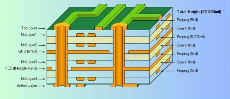
| Layer | Function | Copper Weight | Dielectric Thickness |
|---|---|---|---|
| L1 (Top) | High-Speed Signals | 1 oz | - |
| L2 | GND Plane | 1 oz | 5 mil (Prepreg) |
| L3 | Low-Speed Signals | 1 oz | 18 mil (Core) |
| L4 | PWR Plane | 2 oz | 5 mil (Prepreg) |
| L5 | High-Speed Signals | 1 oz | 18 mil (Core) |
| L6 | GND Plane | 1 oz | 5 mil (Prepreg) |
| L7 | Mixed Signals | 1 oz | 18 mil (Core) |
| L8 (Bottom) | Aux/Test | 1 oz | - |
This table ensures balanced routing density.
Suggested Reading: Unlock Signal Integrity: The Ultimate Guide to 8-Layer PCB Stackup Design
Step 2: Component Placement on 8-Layer PCBs
Placement sets the routing foundation—poor choices inflate trace lengths by 15-20%, hiking losses.
Design Flow:
- Floor Planning: Outline the board; place connectors (RJ45) at edges for accessibility. Group functional blocks: Processor and DDR in the center for short paths (<50 mm to minimize skew).
- Hierarchy: Main ICs first (e.g., PHY chip near Ethernet ports), then passives (decoupling caps 0.1-10 nF within 5 mm of pins). Orient for symmetry—rotate 90° for airflow.
- High-Speed Prioritization: Position DDR4 near its controller; keep analog (e.g., clock gen) 20 mm from digital to cut noise coupling.
- Density Check: Space SMDs at 10-15 mil min (IPC-7351B land patterns); distribute weight evenly to prevent flex.
Reasoning: Proximity reduces propagation delay—e.g., placing caps near PWR pins drops voltage droop below 5%. In multilayer, leverage inner layers for power, freeing top for dense BGA (e.g., 0.8 mm pitch).
Common Pitfall: Clustering high-heat components (processor at 20W) without vias—add thermal reliefs to L4 plane.

Step 3: 8-Layer PCB Routing Techniques
Routing breathes life into placement, especially for high-speed paths where stubs >λ/10 (e.g., 10 mm at 3 GHz) cause reflections.
Design Flow:
- Pre-Route Critical Nets: Assign diff pairs (Ethernet) to L1/L5 with 100 Ω impedance—width 6 mil, spacing 8 mil.
- Layer Hopping: Use blind vias (aspect ratio <8:1 per IPC-6012) for vertical transitions; stitch GND vias every 50 mm.
- Length Matching: Serpentine tune DDR data lines to <50 ps skew; route perpendicular on adjacent layers to slash crosstalk.
- Power Routing: Flood-fill L4 with 10 mil pours; add 20 mil decoupling traces.
High-Speed Focus: For 8-layer, route over solid GND (L2/L6) to confine returns. Grid vias at 15 mil pitch; keep edges 10 mil inset.
Reasoning: Perpendicular routing minimizes coupling—fields decay exponentially. In our router, this keeps eye diagrams open at 2.5 Gbps, per JEDEC JESD79-4 DDR4 specs.

Step 4: 8-Layer PCB Design Rules and Best Practices
Enforce rules via DRC to catch violations early.
Core Rules:
- Trace/Space: 5 mil min for signals, 10 mil for power (IPC-2221B).
- Vias: 8 mil drill, 16 mil pad; blind/buried for density.
- Clearance: 6 mil to planes; 100 mil keep-out for heatsinks.
- Best Practices: Symmetric stackup (mirror L1-L8); AI-optimized paths in 2025 tools for 20% shorter routes. Avoid splits in GND—use fences for isolation.
Reasoning: These guard impedance; e.g., 5 mil traces yield 50 Ω on 5 mil dielectric. For high-speed 8-layer PCB layout, add EMI checks—stitching caps (10 nF) at transitions cut radiation 15 dB.
Incorporate 2025 trends: AI analyzes stackups for thermal hotspots, recommending via arrays that drop temps 25%.
Practical Example: Gigabit Ethernet Router Layout
Apply the flow to our router: Post-schematic import, stackup yields 1.6 mm board with 2 oz PWR. Placement clusters PHY/DDR centrally; routing uses L1 for lanes (matched to 25 ps). DRC flags one via stub—back-drilled to <5 mm. Simulation (HyperLynx) confirms <1% crosstalk. Result: First-pass success, 98% yield.
This example illustrates: Iterative steps + rules = robust high-speed performance.
Conclusion
Mastering 8-layer PCB layout—from stackup symmetry to precise routing—transforms schematics into high-reliability boards. By prioritizing signal-ground adjacency and IPC-compliant rules, you achieve superior integrity for speeds beyond 10 Gbps, while curbing EMI and heat.
In practice, these techniques cut design time and boost yields, especially with emerging AI aids. Next project? Prototype a stackup sketch—it's the gateway to flawless execution. For deeper dives, explore layer simulations early.
FAQs
Q1: What are key 8-layer PCB layout best practices for beginners? A1: Focus on symmetric stackups with signal layers adjacent to GND planes for EMI control (IPC-2221B). Route perpendicular on adjacent layers and match lengths within 50 ps for high-speed nets. Start with floor planning to group components, ensuring decoupling caps within 5 mm of pins—reduces iterations by 25%.
Q2: How do you optimize component placement on 8-layer PCBs? A2: Place main ICs centrally for short paths, orient for airflow, and space SMDs at 10-15 mil (IPC-7351B). Separate analog/digital by 20 mm; add thermal vias under hot components. This minimizes skew and heat buildup, vital for dense high-speed designs.
Q3: What 8-layer PCB routing techniques improve high-speed performance? A3: Use diff pairs with 100 Ω impedance (6 mil width, 8 mil space) on outer layers, over solid GND. Employ blind vias and serpentine tuning for <50 ps skew; stitch edges every 50 mm. Per IPC-2221B, this confines fields, cutting crosstalk below 1% at 2.5 Gbps.
Q4: What are essential 8-layer PCB design rules for impedance control? A4: Maintain 5 mil traces on 5 mil dielectrics for 50 Ω single-ended; ±10% tolerance via DRC. Avoid plane splits and keep edges 10 mil clear. IPC-2221B guidelines ensure stable returns, preventing reflections in multilayer high-speed layouts.
Q5: How does AI impact high-speed 8-layer PCB layout in 2025? A5: AI optimizes routing for 20% shorter paths and flags impedance mismatches in real-time, per 2025 trends. It simulates thermal vias to keep hotspots <85°C, enhancing signal integrity for 5G apps while complying with JEDEC standards.
Q6: Why prioritize stackup in 8-layer PCB design? A6: Symmetric arrangements with 1.6 mm thickness and 5 mil prepregs prevent warpage >0.75% (IPC-6012). It enables precise impedance and EMI shielding, allowing 4 signal layers for complex routing without performance loss.
References
IPC-2221B — Generic Standard on Printed Board Design. IPC, 2012.
IPC-6012E — Qualification and Performance Specification for Rigid Printed Boards. IPC, 2017.
IPC-7351B — Generic Requirements for Surface Mount Design and Land Pattern Standard. IPC, 2010.
JEDEC JESD79-4 — DDR4 SDRAM Standard. JEDEC, 2012.


