Introduction
Designing multi-layer printed circuit boards involves intricate planning of ground and power structures to ensure optimal performance. These structures, often implemented as dedicated planes, play a critical role in maintaining low noise, controlling impedance, and providing stable current return paths. For electrical engineers, understanding the routing strategies and best practices for power and ground planes in multi-layer boards is essential to achieving signal integrity and minimizing electromagnetic interference. This article explores the fundamental principles behind ground and power structures, their routing techniques, and practical guidelines to optimize impedance and reduce noise. By focusing on industry standards and proven methods, we aim to provide actionable insights for engineers working on complex PCB designs.
Why Ground and Power Structures Matter in Multi-Layer Boards
Ground and power structures are foundational elements in multi-layer PCB design. These structures typically consist of dedicated layers, known as planes, that distribute power and provide a reference for signals. Their primary purpose is to ensure a stable voltage supply and a low-impedance path for current return, which is crucial for minimizing noise and maintaining signal integrity. In high-speed or high-frequency applications, improper design of these planes can lead to issues like crosstalk, electromagnetic interference, and signal distortion.
The significance of these structures becomes even more pronounced in multi-layer boards, where multiple signal layers are stacked together. Without well-designed power and ground planes, the risk of interference between layers increases. Additionally, a poorly planned current return path can result in voltage drops and inconsistent performance. For engineers, prioritizing these elements during the design phase directly impacts the reliability and efficiency of the final product.
Technical Principles of Ground and Power Planes
Role of Planes in Impedance Control
Power and ground planes in multi-layer boards are essential for controlling impedance. By placing signal traces adjacent to a continuous ground plane, designers can achieve a predictable characteristic impedance for transmission lines. This setup forms a controlled environment where the electric field between the signal trace and the ground plane remains consistent. Maintaining this impedance is vital for high-speed signals to prevent reflections and ensure data integrity.
The spacing between signal layers and their reference planes also influences impedance. A thinner dielectric layer between the signal and ground plane results in lower impedance, while a thicker layer increases it. Engineers must carefully select stackup configurations to match the required impedance for their specific application, often guided by industry standards like IPC-2221B.
Current Return Paths and Low Noise Design
Current return paths are another critical aspect of ground plane design. In a multi-layer board, the return current from a signal trace typically flows through the nearest ground plane. If this path is interrupted by splits or gaps in the plane, the current must take a longer route, increasing loop area and inducing noise. To achieve low noise, it is necessary to ensure that ground planes are continuous and directly beneath signal traces, especially for high-speed signals.
Noise reduction also depends on minimizing the loop area formed by the signal and its return path. A smaller loop area reduces the potential for electromagnetic interference. This principle is particularly important in mixed-signal designs, where analog and digital signals share the same board. Proper separation of ground planes for different signal types can further enhance low noise performance.
Power Distribution and Decoupling
Power planes distribute voltage across the board, ensuring that components receive a stable supply. However, rapid changes in current demand can cause voltage fluctuations. To mitigate this, decoupling capacitors are placed near power pins of integrated circuits. These capacitors act as local energy reservoirs, smoothing out transient currents and reducing noise on the power plane.
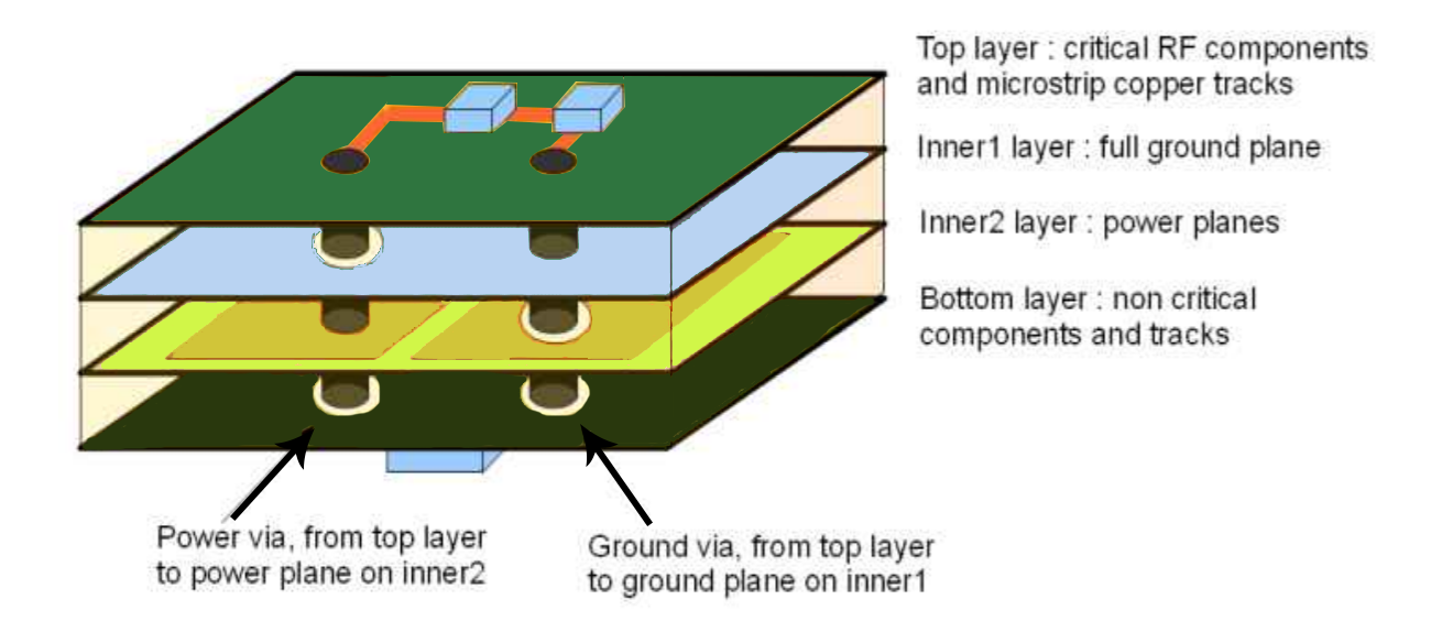
The placement of power and ground planes in the stackup also affects performance. Positioning them as adjacent layers minimizes the distance between them, reducing inductance and improving decoupling effectiveness. This configuration is a standard practice in high-speed designs to maintain a stable power supply under dynamic load conditions.
Best Practices for Routing Ground and Power Structures
Stackup Design for Optimal Performance
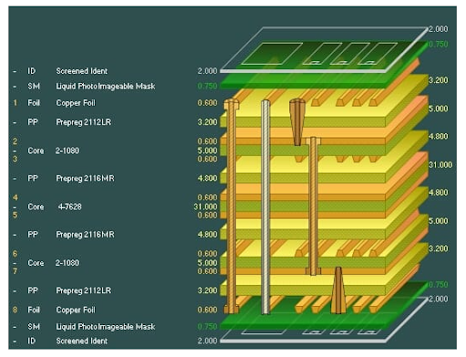
A well-planned stackup is the foundation of effective ground and power routing in multi-layer boards. Engineers should prioritize symmetry in the layer arrangement to avoid warpage during manufacturing. A common stackup for a four-layer board includes signal layers on the top and bottom, with power and ground planes in the middle. For boards with more layers, alternating signal and plane layers can provide shielding and consistent reference planes.
Ground planes should be continuous whenever possible. Avoid splitting ground planes unless absolutely necessary for isolating noisy sections. If splits are required, ensure that signal traces do not cross these gaps, as it disrupts the current return path and increases noise. Standards such as IPC-2221B provide guidelines for layer spacing and material selection to support impedance control and signal integrity.
Routing Techniques for Low Noise
Routing signals in multi-layer boards requires careful consideration of their proximity to ground planes. High-speed signals should be routed on layers adjacent to a ground plane to ensure a direct current return path. Avoid routing over splits or transitioning between layers without maintaining a reference plane, as this can introduce impedance discontinuities.
Differential pairs, commonly used in high-speed designs, benefit from tight coupling and consistent spacing to a reference ground plane. This approach minimizes differential impedance variations and reduces susceptibility to noise. Additionally, keep signal traces as short as possible to limit exposure to interference and reduce loop areas.
Power Plane Design and Decoupling Strategies
When designing power planes, ensure sufficient copper coverage to handle the expected current load. Segmenting power planes into different voltage domains can help manage distribution, but each segment must be adequately decoupled. Place decoupling capacitors close to the power pins of components, with short traces to minimize inductance.
Via placement also plays a role in power distribution. Use multiple vias to connect power and ground planes to component pins, reducing resistance and inductance. This practice is especially important for high-current applications, as outlined in standards like IPC-6012E, which specifies performance requirements for rigid printed boards.
Related Reading: Power Plane Decoupling: A Comprehensive Guide to PCB Stability
Managing Ground Bounce and Crosstalk
Ground bounce occurs when multiple outputs switch simultaneously, causing a temporary shift in ground potential. To mitigate this, ensure that ground planes have low impedance by using a solid, uninterrupted layer. Adding stitching vias around the board’s perimeter can further tie ground planes together across layers, reducing potential differences.
Crosstalk, the unwanted coupling between adjacent traces, can be minimized by maintaining adequate spacing between signal lines and ensuring a nearby ground plane. For critical signals, consider using guard traces connected to ground on either side to provide additional isolation. These techniques align with best practices for high-speed routing and noise reduction.
Troubleshooting Common Issues in Ground and Power Routing
In multi-layer board designs, engineers often encounter challenges related to ground and power structures. One common issue is excessive noise due to improper plane design. If signal traces cross splits in ground planes, the return path becomes longer, increasing noise. To resolve this, review the layout and reroute signals to avoid such crossings, or bridge splits with stitching capacitors if necessary.
Another frequent problem is voltage drop across power planes in high-current designs. This can be addressed by increasing the copper thickness of the power plane or adding more vias for current distribution. Simulation tools can help identify potential bottlenecks before manufacturing, ensuring compliance with performance standards like IPC-A-600K for printed board acceptability.
Thermal management is also a concern, as power planes can generate heat under heavy loads. Ensure adequate copper coverage and consider thermal vias to dissipate heat to other layers or external heat sinks. Following guidelines from standards such as IPC-2221B can help balance electrical and thermal performance.
Related Reading: High Frequency PCB Routing Techniques: Minimizing Signal Loss and Interference
Conclusion
Effective ground and power structures are vital for the performance of multi-layer PCB boards. By focusing on impedance control, low noise design, and proper current return paths, engineers can create robust designs that meet the demands of high-speed and high-power applications. Implementing best practices for stackup design, routing techniques, and decoupling strategies ensures signal integrity and minimizes interference. Adhering to industry standards provides a reliable framework for achieving consistent results. As PCB complexity continues to grow, mastering these principles remains a cornerstone of successful design for electrical engineers.
FAQs
Q1: How do ground planes contribute to low noise in multi-layer boards?
A1: Ground planes provide a stable reference for signals and a direct current return path, reducing loop areas that can induce noise. By maintaining continuity and placing them adjacent to signal layers, interference is minimized. This approach is critical for high-speed designs where noise can degrade performance, ensuring cleaner signal transmission.
Q2: What is the role of power planes in impedance control?
A2: Power planes, when paired with ground planes, help maintain consistent impedance for signal traces by stabilizing the electric field. Proper spacing and dielectric selection between layers, as guided by standards like IPC-2221B, ensure predictable impedance, which is essential for preventing signal reflections in multi-layer designs.
Q3: Why is routing important for current return paths in PCB design?
A3: Routing determines the path signals take relative to ground planes, directly affecting current return efficiency. Poor routing over plane splits disrupts return paths, increasing noise and interference. Proper routing ensures minimal loop areas and maintains signal integrity, especially in high-speed multi-layer boards.
Q4: How can engineers optimize multi-layer stackups for low noise performance?
A4: Engineers can optimize stackups by placing ground planes adjacent to signal layers and avoiding splits under critical traces. Alternating signal and plane layers provides shielding, while symmetry prevents warpage. Following standards like IPC-6012E ensures reliable performance and low noise in complex designs.
References
IPC-2221B — Generic Standard on Printed Board Design. IPC, 2012.
IPC-6012E — Qualification and Performance Specification for Rigid Printed Boards. IPC, 2020.
IPC-A-600K — Acceptability of Printed Boards. IPC, 2020.


