Introduction
High-current PCB design demands careful attention to power integrity and thermal management. Electrical engineers face challenges in balancing manufacturability with performance when components connect to power planes or large copper pours. Thermal relief structures play a critical role in these connections, influencing both soldering processes and operational efficiency. In power delivery networks, where currents exceed several amperes, the choice between thermal relief and direct connections affects resistance, heat dissipation, and overall reliability. This article explores how PCB thermal relief high current applications operate, highlighting trade-offs in power delivery network thermal design. Understanding these impacts ensures robust designs that meet demanding electrical requirements.
What Is Thermal Relief in High-Current PCB Design?
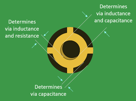
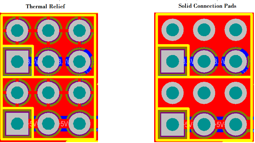
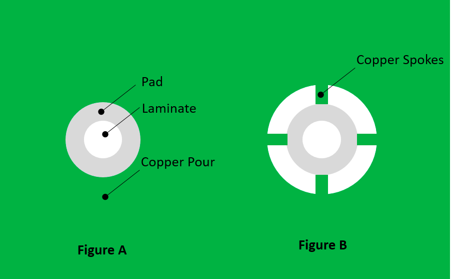
Thermal relief refers to specialized copper connections between component pads and extensive copper areas, such as power planes or pours. Typically, these feature four narrow spokes extending from the pad at 45-degree intervals, creating a thermal barrier during soldering. This design prevents the large copper mass from rapidly dissipating heat from the soldering iron or reflow oven, which could result in incomplete wetting or cold joints. In standard applications, thermal relief enhances assembly yield by allowing localized heating at the pad. For high-current paths, however, the narrowed spokes introduce constraints on current flow and heat transfer. Engineers must evaluate these structures against the needs of power delivery, where low impedance and effective cooling are paramount.
The relevance of thermal relief intensifies in high-current PCBs, where power traces and planes carry sustained loads. Without proper consideration, thermal relief can limit the effective cross-sectional area for current, leading to elevated temperatures. Conversely, omitting reliefs risks assembly defects, particularly in hand-soldering scenarios. Industry practices emphasize context-specific decisions, prioritizing electrical performance in power-intensive sections. This balance directly influences the power delivery network thermal design, ensuring stable voltage rails and minimal losses.
Technical Principles of Thermal Relief Effects
Thermal relief modifies the electrical path by reducing the conductive copper between the pad and plane. Each spoke acts as a narrow trace, typically 0.2 to 0.5 mm wide, summing to less copper than a solid connection. This geometry increases DC resistance slightly, as the effective width narrows compared to a flooded pad. While the resistance rise remains small for signals under 1 A, it accumulates in high-current scenarios, contributing to I-squared-R losses. These losses manifest as localized heating in the spokes, potentially derating the overall current capacity.
From a thermal standpoint, relief structures impede heat flow from the component to the plane. During operation, power-dissipating devices rely on copper planes for spreading heat across the board. The spokes create thermal bottlenecks, reducing conduction to internal layers or heatsinks. This effect proves counterproductive in high-current designs, where components generate significant Joule heating. Direct connections maximize thermal coupling, aligning with principles in IPC-2221 for printed board design. Engineers simulate these paths to quantify temperature rises, ensuring compliance with operational limits.
In power planes, thermal relief for vias or pads further complicates matters. Vias transitioning between layers benefit from solid fills to maintain low impedance across frequencies. Reliefs on these introduce inductance and resistance peaks, degrading power delivery network performance. High-frequency components of the PDN see amplified effects, as spoke geometry acts like a low-pass filter. Balancing spoke count and width becomes essential, with wider spokes mitigating penalties while preserving soldering advantages.
Thermal Considerations for High-Current PCBs
High-current PCBs generate substantial heat from trace and plane resistances, necessitating robust thermal management. Power delivery networks distribute current from sources to loads, relying on low-impedance planes for uniformity. Thermal relief in these networks alters heat distribution, concentrating temperatures at narrowed sections. This localization accelerates electromigration and voids solder joints over time. Standards like IPC-2152 provide charts for trace temperature rise versus current, underscoring the need for adequate copper cross-sections. Narrowed reliefs effectively reduce allowable currents, demanding compensatory measures like thicker copper or parallel paths.
Plane-to-plane coupling via vias exemplifies thermal relief challenges. Filled or staggered vias offer superior paths for both electricity and heat, minimizing hotspots. Applying reliefs here sacrifices interlayer heat spreading, critical for multilayer boards. Engineers assess PDN impedance, where relief-induced resistance spikes correlate with voltage droop under load. Air-cooled systems amplify these issues, as convective cooling struggles with isolated hot spots. Comprehensive thermal modeling reveals these dynamics, guiding relief optimization.
Copper weight influences relief efficacy significantly. Heavier foils, such as 2 oz or more, tolerate narrower spokes due to greater thickness. However, fabrication limits and cost considerations constrain options. In dense layouts, adjacent traces interact thermally, where reliefs disrupt plane continuity and elevate neighboring temperatures. These interactions demand holistic analysis, integrating convection, radiation, and conduction models.
Best Practices for Thermal Relief in Power Delivery
Select connection types based on current levels and assembly methods. For currents below 5 A, standard four-spoke reliefs suffice, easing reflow or hand soldering. Above this threshold, transition to wider spokes or hybrid designs, matching spoke width to upstream trace dimensions. Solid connections suit automated reflow, where uniform heating negates relief needs. Customize rules in design software to apply reliefs selectively to high-current nets.
Optimize spoke geometry for dual electrical and thermal roles. Increase spoke width proportionally to expected current, ensuring collective capacity exceeds requirements per IPC-2152 guidelines. Four spokes at 0.4 mm each handle moderate loads effectively, while six or eight enhance performance. Verify via finite element analysis, focusing on steady-state and transient heating. Incorporate thermal vias arrays near power pads to bypass relief limitations, channeling heat to opposite sides.
Layer stacking impacts relief strategy profoundly. Internal planes provide inherent heat sinking, favoring direct connections for vias. External layers prioritize solderability, where reliefs prevent delamination risks. Maintain clearance rules to avoid shorts during pours. Post-layout verification includes DRC checks and impedance profiles, confirming PDN integrity.
For troubleshooting hotspots, inspect spoke integrity under load. Infrared imaging reveals elevated temperatures indicative of undersized reliefs. Mitigate by rip-up and reroute, or add copper balancing. In production, qualify boards per IPC-6012 specifications, monitoring joint quality post-assembly.
Insights from High-Current Design Simulations
Consider a typical power rail delivering 10 A through a QFN package to a ground plane. Standard reliefs concentrate heat at spokes, raising local deltas by 20-30% over solid pads in simulations. Widening spokes normalizes profiles, aligning with IPC-2152 curves. PDN analysis shows reliefs elevating target impedance above 1 mOhm at low frequencies, risking ripple.
In automotive or industrial applications, cyclic loads exacerbate effects. Direct connections sustain peaks better, distributing stress evenly. Hybrid approaches, blending reliefs with thermal vias, optimize both assembly and runtime. These insights underscore proactive design over reactive fixes.
Conclusion
Thermal relief remains a valuable tool in PCB design, but its application in high-current contexts requires nuance. Narrowed connections trade soldering ease for increased resistance and reduced heat sinking, directly impacting power delivery efficiency. Engineers achieve optimal power delivery network thermal design by sizing spokes appropriately, favoring solids for critical paths, and leveraging standards like IPC-2152 and IPC-2221. Comprehensive analysis ensures reliability under load. Prioritizing these principles yields PCBs that excel in demanding environments, minimizing failures and maximizing performance.
FAQs
Q1: What is the impact of PCB thermal relief high current paths on resistance?
A1: Thermal relief introduces narrow spokes that slightly elevate DC resistance compared to solid pads, primarily by reducing effective copper width. For currents over 5 A, this can lead to higher I-squared-R heating if spokes are undersized. Select wider spokes to maintain low impedance while aiding assembly. Simulations confirm negligible effects below 1 A, but high-current designs demand verification against IPC-2152 guidelines for temperature rise.
Q2: When should you avoid thermal relief for power planes?
A2: Omit thermal relief for power planes in high-current applications exceeding 10 A or where maximal heat dissipation is critical, such as power semiconductors. Direct connections minimize resistance and enhance thermal coupling to internal layers. This applies especially in reflow assembly, where uniform heating suffices. Balance with thermal vias to compensate, ensuring robust power delivery network thermal design.
Q3: How does thermal relief affect power delivery network thermal design?
A3: Thermal relief limits heat conduction from components to planes, creating hotspots in spokes under load. This reduces overall board-level cooling efficiency in high-current PCBs. Opt for optimized geometries or solids to align thermal paths with electrical needs. IPC-2221 principles guide trace sizing, while modeling predicts performance across operating conditions.
Q4: What are best practices for thermal considerations for high current PCBs using reliefs?
A4: Use wider, thicker spokes matched to current capacity, and array thermal vias for bypass. Prefer solids for vias and peaks over 20 A. Qualify per IPC-6012 for joint integrity. These steps preserve power integrity while supporting manufacturability in dense layouts.
References
IPC-2221B — Generic Standard on Printed Board Design. IPC, 2003
IPC-2152B — Standard for Determining Current Carrying Capacity in Printed Board Design. IPC, 2009
IPC-6012E — Qualification and Performance Specification for Rigid Printed Boards. IPC, 2015


