Introduction
If you are an electronic hobbyist dipping your toes into radio frequency projects, high-frequency PCB design tutorial becomes essential for success. Building circuits for WiFi antennas, Bluetooth modules, or even simple radar systems requires more than basic routing skills. At frequencies above 500 MHz, signals behave like waves on transmission lines, leading to issues like reflections and losses if not handled properly. This step-by-step guide breaks down PCB design for RF applications into manageable parts, focusing on signal integrity for beginners. You will learn practical techniques to achieve reliable performance without advanced math. By the end, you can confidently layout boards that minimize errors and maximize efficiency.
What Is High-Frequency PCB Design and Why It Matters
High-frequency PCB design refers to creating printed circuit boards that operate effectively at signal frequencies where the wavelength approaches the physical dimensions of the board or traces. Typically, this starts around 100 MHz and extends into GHz ranges for RF applications. In these regimes, standard low-speed design rules fail because electromagnetic effects dominate, causing signal distortion, crosstalk, and power loss. For hobbyists, understanding this matters when prototyping IoT devices, amateur radio gear, or drone telemetry systems. Poor design leads to weak signals, intermittent failures, or complete project flops. Proper high-frequency practices ensure clean transmission, better range, and compliance with basic performance expectations.
The relevance grows with the rise of wireless tech in home projects. A hobbyist building a 2.4 GHz transceiver might see erratic behavior without controlled layouts. Signal integrity for beginners starts here: treat traces as transmission lines rather than simple wires. This shift prevents common pitfalls like impedance mismatches that reflect power back to the source. Ultimately, mastering these basics elevates your projects from toys to functional tools.
Key Technical Principles in High-Frequency PCBs
At high frequencies, signals propagate as electromagnetic waves along PCB traces, governed by transmission line theory. The characteristic impedance, determined by trace width, thickness, dielectric height, and material properties, must remain constant to avoid reflections. Key parameters include dielectric constant (Dk) for speed and dissipation factor (Df) for loss. Lower Df materials reduce attenuation over distance. Skin effect confines current to the conductor surface, increasing effective resistance and generating heat. These principles form the foundation of PCB layout for high-frequency circuits.
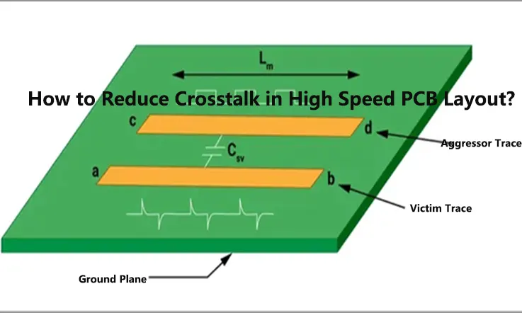
Dielectric losses and conductor losses compound at higher speeds. Radiation occurs if traces act like antennas due to imbalance. Ground bounce and crosstalk arise from shared return paths or proximity. For beginners, visualize signals as water waves: disruptions cause ripples everywhere. IPC-2221 outlines generic design requirements that address spacing and layout to mitigate these effects. Grasping these helps predict and prevent issues early.
Another critical aspect is phase velocity, influenced by the effective Dk. Variations in stackup layers cause skew between signals. Modal dispersion in multi-layer boards further degrades quality. Hobbyists often overlook via transitions, which introduce stubs acting as resonators. Consistent reference planes, either ground or power, provide low-inductance returns. These structured principles guide every design decision.
Step-by-Step Guide to High-Frequency PCB Design
Step 1: Select Appropriate Materials
Start with laminate selection for low-loss performance. Choose materials with stable Dk around 3-4 and Df below 0.005 at your operating frequency. FR-4 works up to 1 GHz but struggles beyond due to higher losses. For RF hobby projects, prioritize thin dielectrics for compact microstrip lines. Consider thermal expansion matching between layers to avoid warpage. Always verify mechanical stability for soldering.
Thickness control is vital; standard 1.6 mm boards suit low frequencies, but thinner cores enable higher impedance control. Prepreg selection fills gaps uniformly. IPC-6018 specifies qualification for high-frequency boards, ensuring reliability under microwave conditions. Test samples if possible, but rely on published datasheets for Dk/Df curves.
Step 2: Design the Stackup
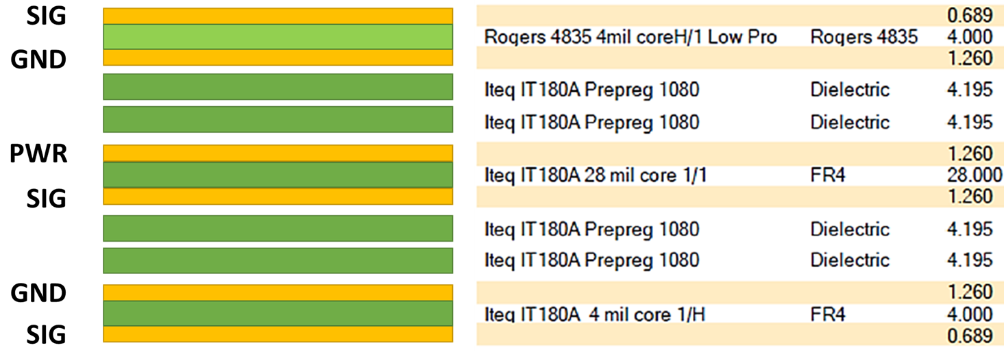
A symmetric stackup prevents twisting and maintains impedance. For four-layer boards, use signal-ground-signal-ground configuration. Core and prepreg thicknesses dictate line spacing. Aim for 50 ohm single-ended or 100 ohm differential pairs common in RF. Simulate stackup early to predict values. Ground planes on adjacent layers shield signals effectively.
Embed microstrip on outer layers for easy probing, stripline internally for isolation. Via fences or stitching grounds reduce slotline modes. Keep power planes away from sensitive signals. This layout strategy supports signal integrity for beginners by minimizing loop areas.
Step 3: Implement Impedance Matching Tutorial
Impedance matching prevents reflections quantified by return loss. Calculate trace width using formulas: for microstrip, width ≈ (height / Z0) * constant adjusted for Dk. Online calculators help beginners without full simulators. Target 50 ohms for most RF inputs. T-junctions or stubs tune mismatches.
For transitions, use tapered lines or series capacitors. Differential pairs require symmetric routing. Verify post-layout with field solvers if available. IPC-2141 provides guidelines for controlled impedance in high-speed designs. Practice on simple couplers first.
Step 4: Route Traces and Optimize Layout
Keep high-speed traces straight with 45-degree bends maximum. Minimize vias; use blind or buried where needed. Length-match critical nets for phase alignment. Flood solid ground planes, avoiding splits under traces. Decouple components close to pins with vias to planes.
Guard traces separate sensitive lines. Component placement groups RF sections away from digital noise. Symmetrical symmetry aids balance. These PCB layout for high-frequency rules reduce EMI. Review for length violations iteratively.
Step 5: Verify Signal Integrity
Check eye patterns conceptually: closure indicates issues. Simulate S-parameters for insertion/return loss. Fabricate test coupons for TDR measurements. Common fixes include widening grounds or adding absorbers. Iterate designs based on prototypes.
Common Challenges and Troubleshooting for Hobbyists
Reflections from unmatched ends cause ringing; add terminations. Crosstalk via coupling needs wider spacing. Vias resonate; back-drill if feasible. Moisture absorbs into dielectrics, shifting Dk; bake boards pre-assembly. EMI leaks from enclosures; shield with pours.
Start simple: single trace tests isolate problems. Oscilloscope probes add capacitance, so use low-loss types. Hobbyist scopes suffice for MHz ranges. Persistent issues trace to ground loops; star-point returns help. Patience yields robust results.
Conclusion
High-frequency PCB design empowers hobbyists to tackle RF challenges with confidence. From material choices to final verification, each step builds signal integrity. Key takeaways include constant impedance, solid grounds, and minimal discontinuities. Apply these in your next project for cleaner signals and better performance. Experiment iteratively, and your boards will shine. This foundation scales to advanced applications seamlessly.
FAQs
Q1: What is the main focus of a high-frequency PCB design tutorial for beginners?
A1: A high-frequency PCB design tutorial emphasizes transmission line effects, impedance control, and layout strategies to maintain signal quality above 500 MHz. Beginners learn to select low-loss materials, design stackups, and route traces without sharp bends. This prevents reflections and losses common in RF hobby projects. Following steps like symmetric planes ensures reliable performance without complex tools.
Q2: How does PCB design for RF improve signal integrity for beginners?
A2: PCB design for RF prioritizes controlled impedance and ground referencing to minimize distortions. Beginners avoid crosstalk by spacing traces and using shielding. Solid reference planes provide return paths, reducing EMI. Simple rules like length matching keep phases aligned. These practices yield stable signals for wireless prototypes.
Q3: Why is impedance matching tutorial crucial in PCB layout for high-frequency?
A3: Impedance matching tutorial teaches calculating trace dimensions for 50-ohm lines, preventing power reflection. In PCB layout for high-frequency, mismatches cause signal bounce and attenuation. Hobbyists use width-height ratios based on stackup. Verification via coupons confirms targets. Proper matching boosts efficiency in RF circuits.
Q4: What are beginner tips for signal integrity for beginners in high-speed traces?
A4: Signal integrity for beginners involves straight routing, via minimization, and decoupling. Place components to shorten critical paths. Flood grounds copiously. Avoid 90-degree corners to curb radiation. Prototype and probe iteratively. These tips make high-frequency hobby projects viable.
References
IPC-2221 — Generic Standard on Printed Board Design. IPC.
IPC-2141 — Controlled Impedance Circuit Boards and High Speed Logic Design. IPC.
IPC-6018 — Qualification and Performance Specification for High Frequency (Microwave) Printed Boards. IPC.


