Introduction
In high-speed PCB design, signal integrity issues such as reflections, crosstalk, and electromagnetic interference dominate the challenges engineers face. Frequencies exceeding several hundred megahertz demand precise control over transmission lines and return paths to prevent performance degradation. Ground plane strategies emerge as a foundational element, providing low-impedance return currents and shielding effects that stabilize signals. These strategies directly influence impedance matching, noise suppression, and overall board reliability. Engineers must prioritize them early in the stackup planning phase to avoid costly redesigns. Proper implementation can significantly enhance data rates in applications like telecommunications and computing systems.
What Are Ground Plane Strategies and Why Do They Matter?
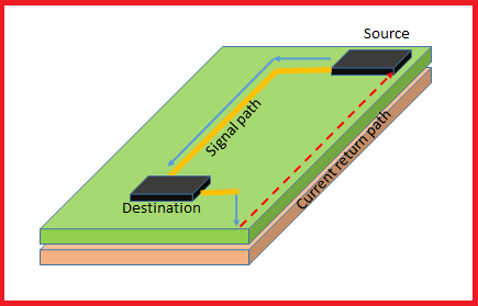
Ground plane strategies involve the strategic placement and configuration of continuous copper pours connected to the ground reference in multilayer PCBs. These planes serve as reference for microstrip and stripline transmission lines, ensuring controlled characteristic impedance. In high-speed designs, they provide the shortest, lowest-inductance path for return currents, which concentrate beneath signal traces due to skin effect at elevated frequencies. Without effective ground planes, return currents spread out, increasing loop inductance and inducing voltage drops that distort signals. This leads to timing errors, bit errors, and compliance failures in eye diagrams.
The relevance intensifies as data rates climb into gigabits per second, where even minor impedance discontinuities amplify jitter. Ground plane strategies also mitigate crosstalk by confining magnetic fields between signal and ground layers. They reduce radiated emissions, aiding electromagnetic compatibility. For electric engineers, mastering these strategies means balancing layer count, material properties, and routing constraints. Poor execution often results in prototypes that pass simulation but fail in real-world testing.
Technical Principles of Ground Plane Strategies
At the core of ground plane strategies lies the principle of minimizing loop area in current paths. In high-speed signals, forward and return currents form a transmission line pair, with the ground plane acting as the return conductor. As per IPC-2221 guidelines on printed board design, wide ground planes ensure uniform current distribution and low inductance. Disruptions like splits or voids force return currents to detour, creating high-inductance loops that generate inductive noise. This noise couples into adjacent traces, exacerbating crosstalk.
Impedance control represents another key mechanism. Microstrip lines, with signals over a ground plane separated by dielectric, achieve 50-ohm impedance through precise trace width, thickness, and dielectric height calculations. Striplines, sandwiched between ground planes, offer superior shielding but require symmetric stackups to avoid mode conversion. Ground planes stabilize these by providing a consistent reference voltage, reducing variations from fabrication tolerances. Engineers calculate effective dielectric constants considering plane proximity.
Electromagnetic shielding further underscores their criticality. A solid ground plane reflects and absorbs fields from high-speed edges, containing emissions within the board. Hatched or meshed planes, used sparingly for thermal relief in power sections, compromise shielding if applied to signal layers. At gigahertz frequencies, plane resonance modes can occur if unstitched, leading to unintended coupling. Thus, strategies must address both DC connectivity and RF behavior.
Best Practices for Ground Plane Strategies in High-Speed PCB Design
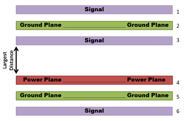
Start with stackup definition, dedicating full ground planes adjacent to every high-speed signal layer. This adjacency ensures tight coupling and minimal inductance, typically aiming for dielectric thicknesses under 0.2 mm where feasible. Route signals exclusively over continuous ground, never crossing splits or power plane edges, to prevent return path lengthening. For multilayer boards, alternate signal and ground planes symmetrically to balance expansion and control warp.
Stitching vias form a cornerstone of robust strategies. Place them every 1/20th of a wavelength along plane edges and splits, calculated from the highest frequency and effective dielectric constant. These vias bridge discontinuities, maintaining plane integrity for return currents. In partitioned designs separating analog and digital sections, connect partitions at a single point near power entry to avoid ground loops while preserving isolation.
Material selection complements plane strategies. Low-loss dielectrics with stable Dk reduce signal attenuation, while plane copper weight affects skin depth at high frequencies. IPC-6012 performance specifications emphasize plane uniformity for qualification, ensuring no voids exceed allowable limits during fabrication inspection. Simulate plane impedance pre-layout using field solvers to verify strategies against target rise times.
For mixed-signal boards, employ guard traces or moats around sensitive areas, tied to local grounds via stitching. Avoid hatched planes under high-speed lines, as slots increase inductance and EMI susceptibility. Verify designs through time-domain reflectometry in prototypes to quantify improvements.
Common Pitfalls in Ground Plane Strategies and Troubleshooting
One frequent error involves splitting ground planes without adequate stitching, causing return currents to loop around the gap and induce crosstalk. Engineers observe this as increased insertion loss or eye closure in simulations. Troubleshooting requires identifying the offending trace via near-end/far-end crosstalk measurements, then adding vias to shorten the path.
Another pitfall arises from routing high-speed signals over power planes, mistaking them for ground references. Power planes carry dynamic currents, injecting noise into signals. The solution lies in reassigning layers or using dedicated grounds. Thermal relief cutouts in planes under bypass capacitors disrupt continuity; minimize them or use solid vias.
In dense boards, via farms near connectors elongate return paths if not fenced with ground vias. Partial ground pours leave islands that float, acting as antennas. Always flood unused areas and connect with multiple vias. Post-fabrication, X-ray inspection reveals plane voids missed in design.
Conclusion
Ground plane strategies stand as indispensable in high-speed PCB design, directly governing signal integrity, EMI performance, and power delivery. By prioritizing continuous planes, precise stitching, and stackup symmetry, engineers mitigate risks inherent to rising frequencies. These practices, rooted in established design principles, yield reliable boards that meet stringent performance margins. Integrating them from concept through verification ensures first-pass success. As designs push boundaries, refining ground plane approaches will remain a competitive edge for electric engineers.
FAQs
Q1: What are the primary ground plane strategies for high-speed PCBs?
A1: Key ground plane strategies include using solid copper pours adjacent to signal layers, implementing stitching vias along edges and splits, and avoiding routing over discontinuities. These ensure low-inductance return paths and controlled impedance. Partitioning for mixed signals requires careful single-point connections to prevent loops. Simulations validate effectiveness before fabrication.
Q2: Why avoid splits in ground planes under high-speed signals?
A2: Splits force return currents to detour, increasing loop inductance and inducing voltage noise that distorts waveforms. This amplifies crosstalk and EMI, especially above 1 GHz. Stitching mitigates this, but prevention through continuous planes proves optimal. Measurements confirm cleaner eye diagrams with unbroken references.
Q3: How do stitching vias enhance ground plane strategies?
A3: Stitching vias provide low-impedance bridges across plane gaps, maintaining current path integrity at RF frequencies. Space them at intervals below 1/20 wavelength of the fastest signal. They also suppress slot resonances. Proper placement reduces insertion loss by several dB in prototypes.
Q4: When might hatched ground planes be acceptable in high-speed designs?
A4: Hatched planes suit power distribution for thermal management but only away from high-speed signals. Under signals, they elevate inductance and EMI. Use solid planes for integrity-critical layers. IPC guidelines favor continuity for performance.
References
IPC-2221B — Generic Standard on Printed Board Design. IPC, 2003
IPC-6012E — Qualification and Performance Specification for Rigid Printed Boards. IPC, 2015
IPC-A-600K — Acceptability of Printed Boards. IPC, 2020


