Introduction
In modern electronics, high-speed PCB designs operate at data rates exceeding several gigabits per second, making signal integrity a critical concern. Signal reflections occur when electrical signals encounter discontinuities along PCB traces, leading to distortions that degrade performance. Engineers must focus on PCB trace impedance control to maintain clean signal propagation and prevent issues like overshoot, ringing, and electromagnetic interference. This article explores the principles behind minimizing reflections through proper transmission line design, impedance matching, and termination techniques. By understanding these elements, designers can ensure reliable operation in high-frequency design environments. Adhering to established guidelines helps achieve robust signal integrity across various applications.
Understanding Signal Reflections and Their Impact on Signal Integrity
Signal reflections arise primarily from impedance mismatches in the transmission path, where the characteristic impedance of the PCB trace differs from the source or load. When a signal travels along a trace longer than one-tenth of the signal wavelength, it behaves as a transmission line, and any discontinuity causes part of the energy to reflect back. This reflected energy superimposes on the original signal, resulting in waveform distortion that compromises signal integrity. Common causes include abrupt changes in trace width, vias, or unterminated ends. In high-speed systems, these reflections can lead to bit errors, increased jitter, and reduced eye diagram opening. Proper management of these effects is essential for maintaining data integrity in demanding circuits.
The relevance of addressing reflections grows with rising clock frequencies and edge rates in processors, memory interfaces, and communication links. Without effective PCB trace impedance control, even short traces can introduce significant degradation at frequencies above 1 GHz. Engineers rely on concepts like return path continuity and ground plane integrity to mitigate these risks. Signal integrity analysis tools simulate these behaviors, but physical design rules form the foundation. Neglecting these principles can result in failed compliance tests or unreliable field performance. Thus, integrating reflection minimization into the initial design phase saves time and resources.
Fundamentals of Transmission Lines in PCB Design
A transmission line in PCB context refers to a controlled-impedance path consisting of a signal trace, reference plane, and dielectric material between them. The characteristic impedance, typically 50 ohms for single-ended or 100 ohms for differential pairs, depends on trace width, thickness, dielectric height, and material properties. According to IPC-2141A, accurate calculation of this impedance requires considering these geometric and material parameters to avoid mismatches. Reflections occur when the reflection coefficient, defined as (Z_L - Z_0)/(Z_L + Z_0), is non-zero at discontinuities. Maintaining uniform impedance along the entire length ensures maximum power transfer and minimal reflections. Designers must model traces as distributed elements rather than lumped circuits for high-frequency design.
Dielectric materials with low loss tangent and stable permittivity support better signal integrity by reducing attenuation and dispersion. Stackup planning plays a key role, as inner layers often provide better impedance control through symmetric stripline configurations. Microstrip traces on outer layers expose signals to air, altering effective dielectric constant and requiring adjustments. Engineers calculate rise time budgets to determine when transmission line effects dominate. Consistent reference planes prevent impedance variations from layer transitions. These fundamentals guide effective high-speed PCB trace design.
Key Factors Causing Signal Reflections
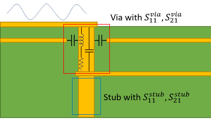
Impedance discontinuities top the list of reflection sources, often from trace bends, pads, or connectors with differing geometries. Vias introduce stubs that act as resonant elements, reflecting energy when stub length approaches a quarter wavelength of the signal frequency. Uncontrolled stub length exacerbates issues in multilayer boards, where through-vias extend beyond the target layer. Branching traces create stubs at split points, further degrading signal integrity. Crosstalk between adjacent traces couples noise, mimicking reflection effects. Identifying these factors early allows targeted mitigation.
Poor return path design disrupts the low-impedance loop for return currents, splitting paths and inducing inductance that amplifies reflections. Ground plane splits or slots force return currents to detour, increasing loop area and EMI susceptibility. In high-frequency design, maintaining a continuous ground plane under signal traces is crucial. Dielectric variations across the board also cause local impedance changes. Fabricators control these through precise material selection and process controls per IPC-2221C guidelines. Addressing all factors holistically ensures comprehensive signal protection.
Best Practices for PCB Trace Impedance Control and Matching
Achieve PCB trace impedance control by defining stackup early and using field solvers for precise calculations based on material datasheets. Target tolerances of 10% or better require tight control over trace etch, dielectric thickness, and copper weight. Symmetric layer stacks minimize warpage and maintain uniform dielectric spacing. Route high-speed signals on inner layers for stripline configurations, which offer superior shielding and impedance stability. Avoid 90-degree bends; use 45-degree or curved transitions to reduce reflections. Length-matching critical nets preserves timing integrity alongside impedance.
Impedance matching starts at the driver and receiver, ensuring source and load impedances align with trace Z0. Differential pairs demand equal lengths and tight coupling, with ground or power planes as references. Maintain consistent spacing to adjacent traces to control crosstalk. Reference planes should extend beyond trace edges by at least three times the dielectric height. These practices form the core of robust high-frequency design.
Termination Techniques to Minimize Reflections
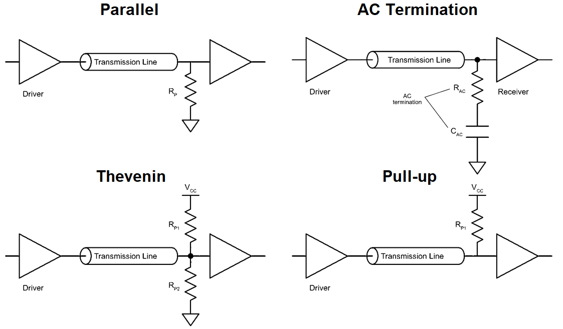
Termination techniques absorb incident signals, preventing reflections from open or shorted ends. Series termination places a resistor near the driver, matching source impedance to Z0 and damping initial reflections. Parallel termination at the receiver uses a resistor to ground or supply, sized to Z0 for multi-drop buses. AC termination employs a resistor-capacitor network, reducing DC power while providing high-frequency matching. Thevenin termination combines series and parallel resistors to emulate source impedance. Selection depends on topology, loading, and power budgets.
For point-to-point links, series termination suffices with minimal components. Multi-drop buses benefit from parallel or AC schemes to handle reflections from multiple loads. Minimize stub length to termination points, ideally under one-twentieth of the rise time distance. Simulate termination values to optimize eye patterns. Proper implementation significantly enhances signal integrity.
Optimizing Return Path and Ground Plane for Signal Integrity
A solid return path completes the transmission line loop, carrying return currents directly beneath signal traces. Continuous ground planes provide the lowest inductance path, minimizing voltage drops and reflections. Avoid splits under high-speed nets; bridge gaps with stitching vias if unavoidable. Power planes can serve as returns if decoupled properly, but dedicated ground layers offer cleaner performance. In multilayer boards, assign adjacent layers for signal-ground pairs.
Ground plane integrity reduces common-mode noise and improves EMI performance. Fill unused areas with ground to stabilize references. Via fences along trace edges enhance shielding for sensitive signals. These strategies complement impedance control for overall signal integrity.
Troubleshooting Reflections in High-Frequency Designs
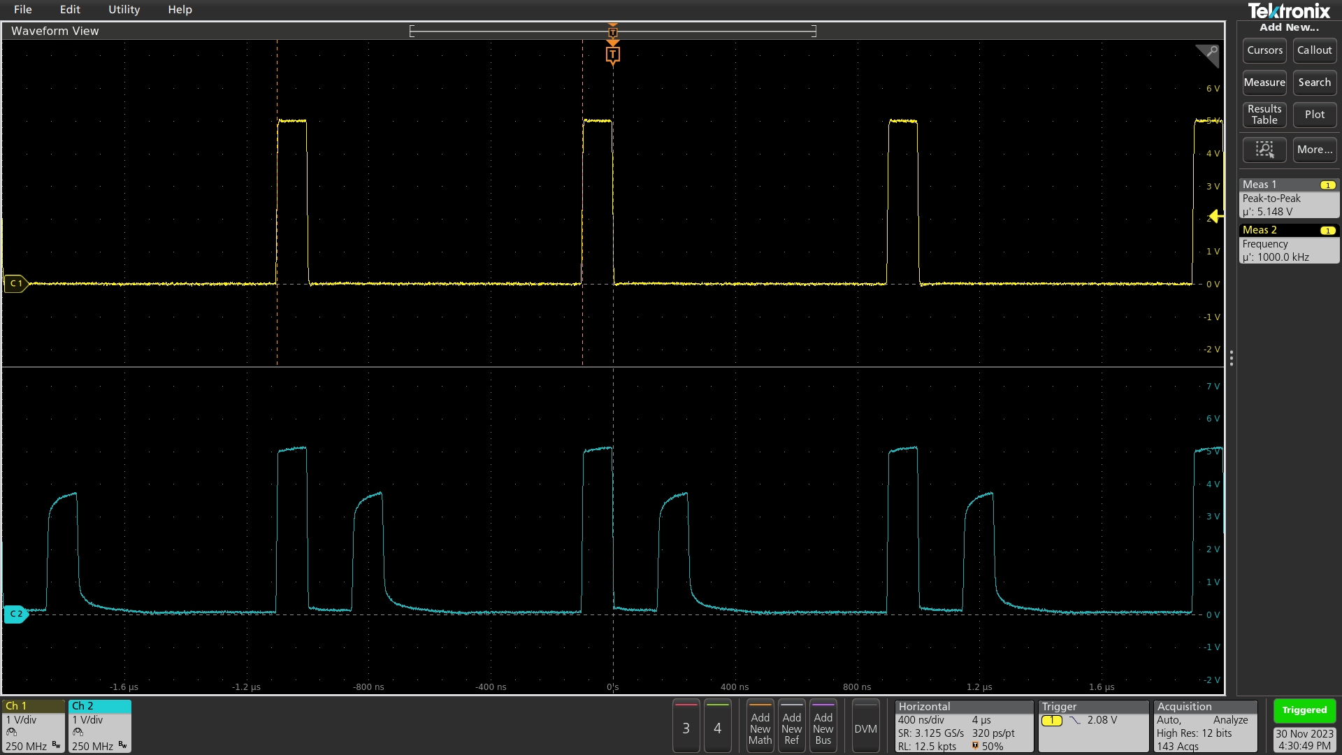
Common symptoms include ringing on edges, closed eye diagrams, or excessive jitter in measurements. Use time-domain reflectometry to locate discontinuities by observing impedance steps. Frequency-domain sweeps reveal stub resonances as nulls in insertion loss. Simulate stackups and routing to correlate with measurements. Adjust trace geometries iteratively within tolerances.
Fabrication variations like etch non-uniformity require design margins. Post-layout verification against IPC-6012E performance specs ensures compliance. Systematic troubleshooting isolates issues efficiently.
Conclusion
High-speed PCB trace design demands meticulous attention to transmission line principles, PCB trace impedance control, and impedance matching to minimize signal reflections. Implementing termination techniques, limiting stub length, and ensuring robust return paths and ground planes form the pillars of signal integrity. Logical adherence to these practices, informed by standards like IPC-2141A and IPC-2221C, yields reliable high-frequency designs. Engineers benefit from structured approaches that balance performance and manufacturability. Prioritizing these elements from concept to fabrication guarantees success in demanding applications.
FAQs
Q1: What role does PCB trace impedance control play in signal integrity?
A1: PCB trace impedance control maintains consistent characteristic impedance along transmission lines, preventing mismatches that cause reflections. In high-frequency design, this ensures clean signal propagation, reduces jitter, and opens eye diagrams. Designers calculate widths and layer spacing precisely to achieve targets like 50 ohms single-ended. Proper control aligns with industry guidelines for reliable performance.
Q2: How do termination techniques improve impedance matching?
A2: Termination techniques match source or load impedances to the transmission line Z0, absorbing signals to eliminate end reflections. Series termination near drivers damps ringing effectively for point-to-point nets. Parallel or AC methods suit loaded buses by providing broadband matching. Selecting the right type based on topology enhances overall signal integrity.
Q3: Why is minimizing stub length critical in high-speed PCB design?
A3: Stub length in vias or branches acts as a resonator, reflecting energy at quarter-wavelength frequencies and degrading signal integrity. Keeping stubs shorter than one-tenth the rise time distance avoids resonances. Backdrilling or blind vias reduce effective length in multilayer boards. This practice preserves return path continuity and bandwidth.
Q4: How does a ground plane support return path in signal integrity?
A4: A continuous ground plane provides a low-inductance return path directly under traces, minimizing loop inductance and reflections. It stabilizes reference impedance and shields against crosstalk. Stitching vias bridge any splits, ensuring current flows efficiently. Solid ground planes are foundational for high-frequency design success.
References
IPC-2141A — Design Guide for High-Speed Controlled Impedance Circuit Boards. IPC, 2004
IPC-2221C — Generic Standard on Printed Board Design. IPC, 2023
IPC-6012E — Qualification and Performance Specification for Rigid Printed Boards. IPC, 2017


