Why Is Component Spacing So Critical in High-Voltage PCB Design?
Designing printed circuit boards that handle high voltages demands meticulous attention to detail, primarily to avert the dangerous phenomenon of electrical arcing. Arcing, defined as an abrupt discharge of electricity through an insulating medium like air between conductive elements, poses significant risks. These risks include component damage, short circuits, and even the potential for fires. The most effective strategy to prevent such incidents involves ensuring ample spacing between components and traces that carry high voltages. This adequate spacing on high-voltage PCBs ensures that the electric field strength between conductors remains below the breakdown voltage of the surrounding dielectric, typically air or the PCB substrate.
Beyond immediate safety concerns, proper spacing profoundly influences the overall performance and reliability of the circuit board. Insufficient spacing can lead to undesirable effects such as electromagnetic interference (EMI), signal crosstalk, or unintended parasitic capacitance between traces. By diligently adhering to established high-voltage PCB layout guidelines, designers can substantially mitigate these risks, resulting in designs that are both safe and highly efficient.
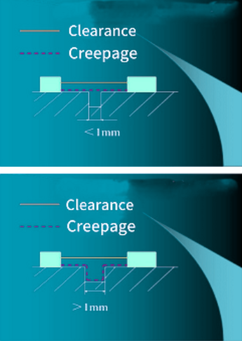
Understanding Clearance and Creepage
Before delving deeper into layout strategies, it's crucial to clarify two fundamental concepts related to spacing in high-voltage PCB design:
● Clearance: This refers to the shortest distance measured directly through the air between two conductive elements. Clearance is paramount for preventing immediate arcing in designs exposed to high voltages.
● Creepage: This is defined as the shortest path measured along the surface of an insulating material between two conductive elements. Creepage distance is particularly important for preventing surface discharges, especially when the PCB operates in humid or contaminated environments.
Both clearance and creepage distances must be meticulously calculated, taking into account the operating voltage levels, anticipated environmental conditions, and adherence to relevant industry standards such as IPC-2221 or IEC 60950. For instance, a circuit operating at 500V might typically require a clearance of about 2.5 mm, whereas the creepage distance could necessitate 3.2 mm or more, contingent on the specific insulating material and the expected degree of environmental pollution.
What Are the Core Principles for Spacing Components on High-Voltage PCBs?
Optimizing component spacing on high-voltage PCBs requires a balanced approach, weighing safety imperatives against functional requirements and manufacturability. Adhering to specific core principles during layout is essential to prevent arcing and guarantee long-term reliability.
Complying with Voltage-Specific Spacing Standards
The necessary separation between components and traces must be directly proportional to the voltage levels present in your circuit; higher voltages inherently demand greater distances to prevent dielectric breakdown. Industry standards provide precise minimum spacing guidelines. For example, IPC-2221B suggests a clearance of at least 0.25 mm per 100V for voltages between 301-500V, implying a 1.0 mm clearance for a 400V differential under ideal conditions. However, for critical safety applications, these values are frequently doubled or adjusted to account for factors like altitude and specific environmental conditions. It is imperative to consult the precise standards applicable to your project. Over-spacing can lead to an unnecessarily larger board footprint, while under-spacing introduces significant risks of arcing and operational failure. Design software equipped with integrated Design Rule Checks (DRC) is invaluable for enforcing these critical spacing rules throughout the layout process.
Accounting for Environmental Factors
The operational environment of the fast turn PCB profoundly influences spacing requirements. Factors such as high humidity, airborne dust, or other pollutants can significantly diminish the insulating properties of both air and surface materials, thereby elevating the risk of arcing or surface discharge. In such challenging conditions, creepage distances must be increased accordingly. For instance, in an industrial setting classified as pollution degree 2, a 500V application might necessitate creepage distances of 4.0 mm or greater, a considerable increase compared to the 2.5 mm required in a clean, controlled environment. Altitude also plays a role in clearance distances, as reduced air pressure at higher elevations lowers air's dielectric strength. Designs intended for operation above 2000 meters may require an increase in clearance distances by 10-20% to compensate for this effect.
Strategic Component Grouping and Edge Smoothing
An effective strategy for component placement on high-voltage PCBs involves grouping components according to their operational voltage levels. By segregating high-voltage components and traces from low-voltage sections, the risk of arcing across large potential differences is significantly minimized. For example, high-voltage power transistors or capacitors should be located in a distinct area of the board, while control circuitry or low-voltage signal paths are isolated in another. Where necessary, physical barriers such as milled slots or specialized insulating materials can be integrated to further enhance the separation of these zones. Additionally, sharp edges or pointed traces can create localized concentrations of electric fields, significantly increasing the probability of arcing. During high-voltage PCB layout, it is best practice to use rounded corners for traces and pads whenever feasible. This approach disperses the electric field more uniformly, effectively reducing voltage stress and the potential for breakdown.
Key Layout Guidelines for Arc Prevention in High-Voltage PCBs
Transitioning from fundamental principles, specific high-voltage PCB layout guidelines are crucial for designing boards that are both inherently safer and reliably perform under stress. These practical steps, implemented during the design phase, are fundamental to preventing arcing and optimizing overall board performance.
Optimal Trace Design for High Voltages
High-voltage traces frequently carry substantial electrical currents, leading to heat generation and an increased risk of dielectric breakdown if the traces are too narrow. Wider traces not only manage current more effectively but also facilitate greater spacing from adjacent conductors. A general guideline suggests that for every 1A of current, a trace on a standard 1 oz copper layer should be at least 0.5 mm wide. For high-voltage applications, further increasing this width is advisable to minimize resistance and heat accumulation, thereby enhancing safety margins. Furthermore, placing components directly underneath high-voltage traces or pads can inadvertently create short paths for arcing, particularly under mechanical stress or contamination. It is essential to route high-voltage traces away from sensitive components; if crossing is unavoidable, consider using inner layers or implementing effective shielding. When components must be in close proximity to high-voltage areas, stringent adherence to clearance and creepage distance requirements is paramount.
Implementing Physical Isolation and Dielectric Testing
For designs involving extremely high voltages (exceeding 1000V), incorporating physical barriers such as slots or cutouts within the PCB itself can significantly increase creepage distances. Slots are particularly effective when placed between high-voltage pads or traces, as they compel any surface discharge to follow a much longer, safer path. For instance, a 1.6 mm slot separating two pads rated for 1500V can substantially reduce arcing risks. Additionally, applying insulating materials or conformal coatings can provide an extra layer of protection. After the layout is complete, it's vital to simulate or physically test the dielectric strength of your PCB materials and the chosen spacing. Standard PCB FR-4 material typically has a dielectric strength of approximately 20 kV/mm, though this can fluctuate based on manufacturing quality and environmental conditions. Ensure that your design does not push the material beyond its rated limits. For critical applications, consider specialized high-voltage laminates, such as polyimide-based materials, which offer superior dielectric strength.
Best Practices for Component Placement in High-Voltage Designs
Effective component placement on high-voltage PCBs works synergistically with proper spacing to prevent arcing and ensure a robust design. Adhering to these best practices during the layout phase is crucial.
Thermal Management and Consistent Spacing
Components handling high voltages, such as power transistors or diodes, often generate considerable heat. Positioning these elements in areas with excellent airflow or adjacent to heatsinks is critical to prevent thermal buildup, which can degrade insulation and heighten the risk of arcing. It's advisable to avoid clustering heat-generating components unless sufficient cooling solutions are specifically provided. Furthermore, maintaining consistency in spacing rules across the entire board is essential to eliminate potential weak points in your design. Utilize design software to establish and enforce uniform clearance and creepage rules for all high-voltage nets. For example, if a 3 mm clearance is mandated for a 600V section, this rule should be consistently applied to all relevant traces and components to minimize errors and ensure predictable performance.
Isolating Sensitive Circuitry
Sensitive components, such as microcontrollers or various sensors, are particularly vulnerable to electrical noise and voltage spikes. These should be strategically placed away from high-voltage areas to prevent interference and potential damage. If space constraints necessitate their proximity, employ robust shielding techniques or utilize optocouplers to achieve effective electrical isolation between high-voltage and low-voltage domains, thus safeguarding critical control circuitry.
Common Pitfalls to Avoid in High-Voltage PCB Layout
Even seasoned designers can encounter challenges when developing high-voltage PCBs. Being aware of prevalent mistakes, particularly concerning component spacing and layout, can significantly enhance design reliability.
Overlooking Creepage and Manufacturing Tolerances
A frequent oversight is prioritizing clearance distances while underestimating the importance of creepage, especially in environments prone to humidity or contamination. Always calculate creepage distances based on the anticipated operating conditions and the specific properties of the insulating materials. Neglecting this can lead to surface discharges, which compromise the board's safety and longevity. Additionally, a design that theoretically meets spacing requirements may fail in production due to manufacturing tolerances. For instance, a theoretical 2.0 mm trace-to-trace clearance could be reduced to 1.8 mm during etching. It is crucial to factor in these tolerances by incorporating a safety margin, typically 10-20%, into your spacing rules.
Dangers of Board Overcrowding
Attempting to shrink board dimensions by excessively compacting components is a critical error that can lead to inadequate spacing and an elevated risk of arcing. While compact designs are often desirable, safety must always take precedence in high-voltage applications. Allocate sufficient space for proper component spacing, even if it necessitates a larger board footprint, to ensure reliability and compliance with safety standards.
Conclusion: Achieving Safer High-Voltage PCBs Through Precise Spacing
Optimizing component spacing on high-voltage printed circuit boards stands as a foundational step in preventing electrical arcing and assuring the unwavering safety and reliability of your designs. By diligently adhering to voltage-specific spacing standards, carefully considering environmental influences, and implementing proven high-voltage PCB layout guidelines, designers can dramatically mitigate risks. This approach leads to the creation of boards that consistently perform even under the most demanding operational conditions. Thoughtful component placement in high-voltage PCB designs, coupled with practical strategies such as incorporating physical slots or utilizing wider traces, further fortifies the design’s inherent robustness.
Whether your work involves power supplies, complex industrial equipment, or cutting-edge renewable energy systems, mastering the nuances of component spacing for high-voltage PCBs is an invaluable skill. This expertise directly translates into the development of safer, more efficient designs. Dedicate the necessary attention to apply these principles in your next project, and you will be well-equipped to produce high-performing, arc-free PCBs that are built to last.


