What is PCB trace spacing and why does it matter?
Trace spacing refers to the precise distance maintained between conductive paths, or "traces," on a printed circuit board. Achieving the correct spacing is not merely a design preference; it is a fundamental requirement for preventing a range of electrical problems. Insufficient spacing can lead to critical issues such as short circuits, electrical arcing, and unwanted signal interference.
Conversely, allocating excessive space between traces can result in an inefficient use of valuable board real estate. This balance is crucial because accurate trace spacing directly influences the board's safety, its electrical performance, and its overall operational reliability. Properly calculated spacing ensures that the PCB functions as intended throughout its lifespan.
How does trace spacing impact PCB performance and safety?
The distance separating traces profoundly affects several critical aspects of a PCB's operation. Firstly, for safety, adequate spacing is vital in preventing hazardous short circuits and electrical arcing, especially in systems handling high voltages where safety compliance is non-negotiable. Secondly, signal integrity benefits immensely; proper spacing mitigates crosstalk and electromagnetic interference (EMI), thereby ensuring that signals remain clear, stable, and accurate.
Lastly, manufacturability is also a key consideration. Trace spacing must align with the capabilities of the PCB fabrication process. Designs that fail to account for manufacturing tolerances can lead to production errors and increased PCB cost. For these reasons, meticulously calculating trace spacing is not merely a recommendation but an essential step in robust PCB design.
What's the difference between clearance and creepage in PCB design?
Before delving into specific calculations, it's important to differentiate between two fundamental concepts often discussed when determining trace spacing: clearance and creepage. Both are critical for ensuring the electrical safety and long-term reliability of a PCB, particularly in environments where voltage levels or contaminants are a concern.
What is electrical clearance on a PCB?
Clearance defines the shortest distance measured through the air between two uninsulated conductive elements on a PCB. Its primary purpose is to prevent electrical arcing, which occurs when electricity jumps across an air gap. This phenomenon is more likely to happen in high-voltage circuits. For example, a circuit operating at 50V DC might need a minimum clearance of 0.6 mm to prevent arcing under normal operating conditions. Factors like altitude and humidity can influence the required clearance, as they affect the air's dielectric strength.
What is electrical creepage on a PCB?
Creepage, in contrast, refers to the shortest distance between two conductive parts measured along the surface of the insulating material of the PCB. This distance is vital for preventing "surface tracking," a process where a conductive path gradually forms on the board's surface due to contamination (like dust or moisture) and sustained voltage. For instance, a 100V application might require a creepage distance of 1.25 mm, but this can vary significantly based on the PCB material's comparative tracking index (CTI) and the potential environmental pollution level.
What factors influence the required trace spacing?
Determining the optimal trace spacing is not a one-size-fits-all solution; it depends on a confluence of design and environmental variables. Each of these factors plays a crucial role in dictating the minimum safe and effective distances between conductive paths on a PCB.
Key design and environmental variables
The voltage levels present in different parts of the circuit are perhaps the most significant factor. Higher voltages necessitate greater spacing to prevent arcing and ensure safety. For instance, a 500V circuit will demand considerably more clearance than a 5V logic circuit. Environmental conditions, such as humidity, dust accumulation, and even altitude, can also impact electrical behavior, often requiring increased spacing in harsher settings to account for potential conductive contaminants or reduced air density.
The type of PCB material used is another critical consideration, particularly for creepage distances. Materials with lower comparative tracking index (CTI) values are more susceptible to surface tracking and thus require larger creepage distances. Finally, the specific application type, whether it’s a high-speed digital interface or a robust power electronics module, will influence spacing. High-speed signals might prefer tighter spacing to control impedance, while power circuits prioritize safety and heat dissipation with wider gaps.
How can you accurately calculate PCB trace spacing?
Calculating the appropriate trace spacing involves a systematic approach that combines an understanding of electrical principles with adherence to industry standards and the practical use of digital tools. This method ensures both safety and optimal performance for your circuit board.
A step-by-step approach to calculating trace spacing
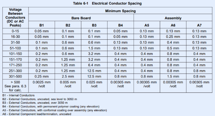
Begin by clearly identifying the voltage levels present across different sections of your PCB design. Differentiate between low-voltage signals and high-voltage power lines, as this directly influences the required clearance and creepage. Next, consult established industry standards, such as IPC-2221 or IEC 60950, which provide detailed guidelines and tables for minimum spacing based on voltage, environment, and material properties. These standards are your primary reference for safe design practices.
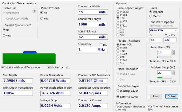
For efficient and precise calculations, utilize online tools like a PCB clearance calculator or a PCB creepage calculator. These digital aids allow you to input your specific design parameters—such as voltage, board material, and environmental conditions—and receive recommended spacing values that align with industry benchmarks. Finally, it's crucial to confirm that your calculated spacing dimensions are compatible with your chosen PCB manufacturer's capabilities. Manufacturing tolerances can vary, so verify that your design’s minimum spacing requirements are achievable within their production process to avoid costly redesigns or production delays.
What tools simplify trace spacing calculations?
While understanding the principles of trace spacing is vital, modern PCB design benefits immensely from specialized digital tools that streamline calculations and enhance accuracy. These resources help engineers quickly determine optimal spacing without extensive manual computations.
Digital aids for precise PCB design
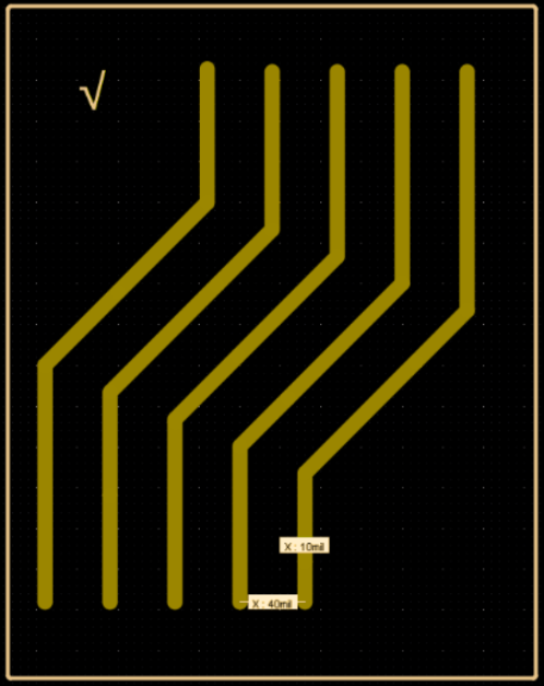
One readily available resource is the online trace spacing tool. These web-based calculators enable designers to input parameters like voltage and material type, instantly yielding recommended spacing values based on industry standards. They are excellent for preliminary checks and ensuring compliance. For situations specifically focused on preventing arcing, a dedicated PCB clearance calculator is indispensable, helping to determine the minimum air gap distances.
Similarly, a PCB creepage calculator specializes in surface distances, factoring in insulation materials and environmental conditions to provide precise creepage values. These tools remove much of the guesswork from the design process, allowing engineers to focus on other complex aspects of the PCB layout. Many of these calculators are freely accessible and user-friendly, making them valuable for both novice and experienced designers.
Practical advice for optimizing trace spacing
Beyond the foundational calculations, several strategic design practices can further refine trace spacing, contributing to a more robust, reliable, and manufacturable PCB. Implementing these tips can help mitigate potential issues and enhance overall board performance.
Best practices for efficient PCB layouts
To minimize interference and simplify spacing, group traces with similar voltage levels or signal types together. For instance, keep high-voltage power traces spatially separated from sensitive low-voltage data lines. The strategic use of a robust ground plane is also highly effective; a well-designed ground plane can significantly reduce electromagnetic interference (EMI) and crosstalk, potentially allowing for tighter spacing in certain digital circuit areas without compromising signal integrity.
Consider applying a conformal coating to your PCB. This protective layer can substantially reduce the required creepage distances by safeguarding the board surface from moisture and contaminants, which are primary contributors to surface tracking. Lastly, integrate simulation software into your design workflow. Running signal integrity and power integrity simulations can help identify potential issues related to trace spacing early in the design phase, allowing for adjustments before PCB prototype manufacturing.
Avoiding common errors in trace spacing
Even with advanced tools and established guidelines, certain missteps in trace spacing calculations can lead to design flaws and operational failures. Being aware of these common mistakes is crucial for developing reliable PCB layouts.
Critical pitfalls to steer clear of
A frequent error is basing spacing calculations solely on nominal operating voltages while neglecting transient voltage peaks. These momentary, higher voltage spikes can occur and require larger spacing to prevent arcing, so always account for the maximum anticipated voltage. Another common oversight is failing to adequately consider the operating environment; factors like high humidity, dust, or even varying altitudes can alter electrical behavior and demand increased spacing to prevent breakdowns.
Designers sometimes overlook adherence to industry standards such as IPC-2221. These standards are not merely suggestions; they are critical benchmarks for ensuring safety and reliability. Always cross-reference your design against these guidelines. Finally, avoid the assumption that uniform spacing applies across the entire board. Different sections of a PCB, particularly those handling high-speed signals, high voltages, or sensitive analog signals, will necessitate varying trace spacing requirements tailored to their specific functions and potential interference risks.
Concluding thoughts on mastering PCB trace spacing
Accurately determining trace spacing is a cornerstone of effective PCB design, directly influencing the board's safety, its functional performance, and its ease of manufacturing. By developing a clear understanding of concepts like electrical clearance and creepage, and by systematically factoring in variables such as voltage levels, environmental conditions, and material properties, engineers can establish reliable spacing parameters. Leveraging specialized tools—including online trace spacing calculators, PCB clearance calculators, and PCB creepage calculators—further enhances precision and ensures compliance with industry standards.
Whether you are configuring a simple low-voltage control board or engineering a complex high-voltage power supply, the detailed guidance provided here offers a practical framework for achieving optimal trace spacing. Through diligent planning, the strategic application of these principles, and the use of appropriate resources, designers can produce PCB layouts that are inherently safe, highly efficient, and primed for successful production. AIVON is dedicated to supporting your design endeavors with comprehensive resources and expert insights. Use this guide as a foundation to refine your trace spacing calculations, thereby elevating the overall quality and reliability of your PCB projects.


