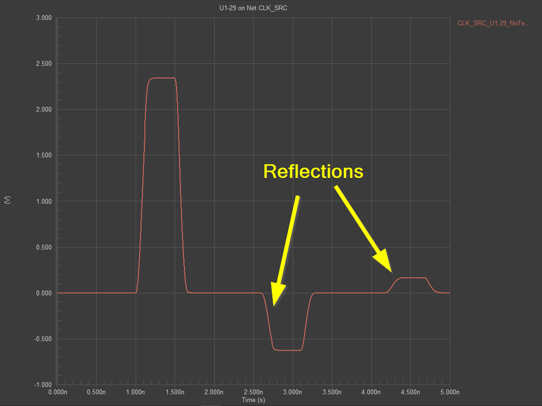
Signal reflection occurs whenever a transmitted wave encounters an impedance discontinuity along its path. In high-speed digital and RF designs, these reflections create ringing, overshoot, undershoot, and bit errors that limit maximum reliable data rate. The most effective solution is to implement controlled impedance from source to load so every segment of the transmission line presents the same characteristic impedance. This article explains the mechanisms of reflection and presents practical, field-proven methods to minimize it through proper PCB impedance design.
Understanding Signal Reflection
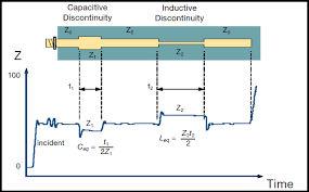
Reflection coefficient Γ at any interface is defined as:
Γ = (Z₂ − Z₁) / (Z₂ + Z₁)
Where Z₁ is the characteristic impedance of the transmitting line and Z₂ is the impedance seen at the discontinuity. When Γ = 0 (Z₁ = Z₂), no reflection occurs and the signal travels cleanly forward.
Common sources of mismatch on PCBs
- Trace width changes
- Via transitions
- Layer changes without proper reference
- Incorrect termination
- Package pin capacitance
- Connector impedance deviation
Key Methods to Reduce Signal Reflection
1. Design All Critical Traces as Controlled-Impedance Lines
Route high-speed interfaces (USB, HDMI, DDR, PCIe, Ethernet) with target impedance specified in the fabrication notes.
- 50 Ω single-ended
- 90–100 Ω differential
- 60–75 Ω for some RF applications
2. Maintain Continuous Reference Planes
Every impedance-controlled trace must have an unbroken solid reference plane (GND or PWR) directly underneath or above it.
Avoid:
- Crossing splits in reference planes
- Routing over large voids or cutouts
- Changing reference plane without stitching vias
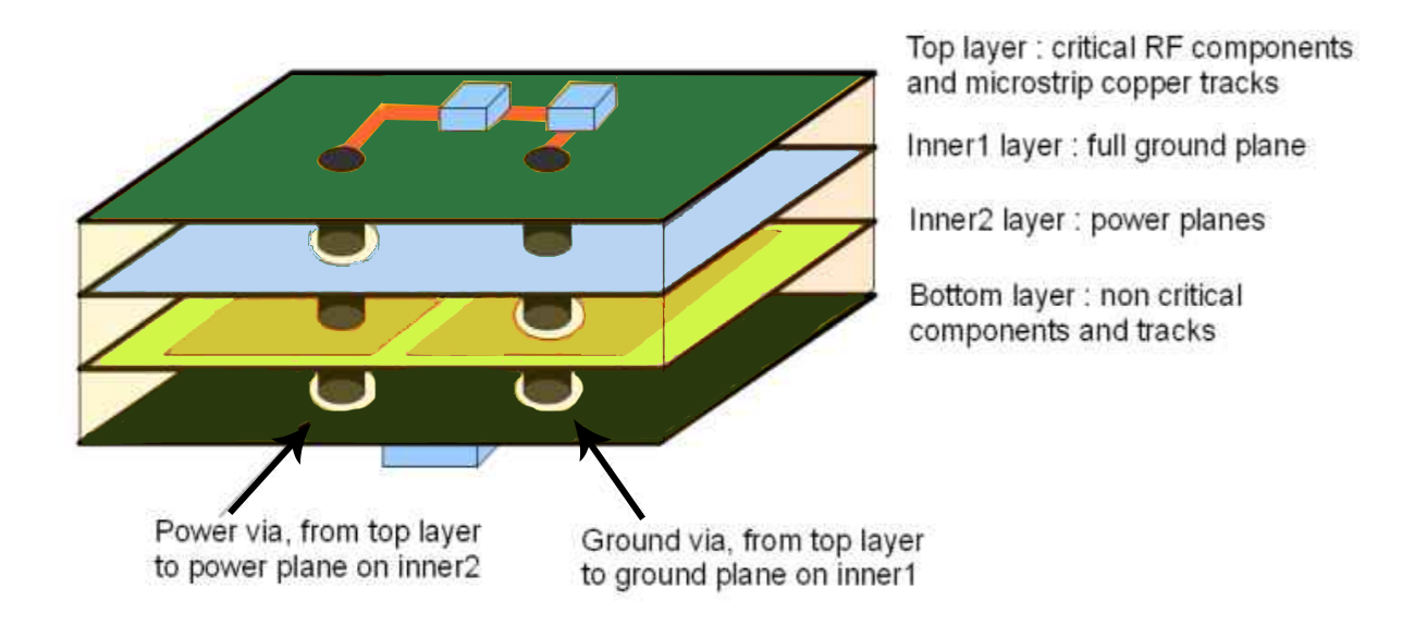
3. Use Proper Via Transitions
- Place ground return vias immediately adjacent to signal vias (within 0.5 mm)
- Use back-drilled or blind vias when stub length exceeds λ/20
- Keep via antipad size minimal to reduce capacitance discontinuity
Suggested Reading: Backdrilling and Blind Vias: A Combined Approach to Signal Integrity
4. Implement Correct Termination Strategies
Interface | Recommended Termination | Purpose DDR3/4 | ODT + VTT termination | Eliminate reflections at memory LVDS / USB2 | 100 Ω parallel at receiver | Match differential impedance Single-ended clock | 33–47 Ω series at source | Reduce source-end reflection PCIe / USB3 | AC coupling + receiver bias | Block DC, maintain impedance
5. Optimize Trace Geometry
- Keep trace width constant throughout the route
- Use smooth 45° angles instead of sharp 90° corners
- Maintain consistent spacing in differential pairs
- Avoid neck-down sections longer than 3 mm
Practical Impedance Control Workflow
- Determine required impedance from datasheet or standard (e.g., USB 2.0 = 90 Ω ±15 %)
- Select stack-up with appropriate dielectric thickness to reference plane
- Calculate trace width using fabricator’s impedance calculator or field solver
- Add impedance control coupons to the panel
- Specify target impedance and tolerance (±10 % typical) in fabrication drawing
- Verify with TDR testing on first article
Suggested Reading: The Impact of Impedance Control on Crosstalk: A Comprehensive Analysis
Layer Transition Best Practices
- Place two ground vias for every signal via in differential pairs
- Keep total transition length < 5 mm
- Mirror the trace geometry on both layers
- Route perpendicular to the previous direction for only a short distance
Real-World Results
A 4 Gbps PCIe Gen3 design with poor plane referencing showed 600 mV ringing and frequent CRC errors. After implementing continuous ground reference, proper via stitching, and source-series termination, eye height improved from 120 mV to 420 mV and bit error rate dropped below 10⁻¹².
Conclusion
Signal reflection is completely preventable through disciplined impedance design. The combination of correct stack-up planning, continuous reference planes, proper via management, and appropriate termination eliminates ringing and enables reliable operation at the highest data rates supported by modern silicon. Controlled impedance is not an optional luxury; it is a fundamental requirement for any design operating above 100–200 MHz.
FAQs
Q1: When do I really need controlled impedance traces?
A1: Any signal with rise time faster than approximately 1 ns (most modern logic families) or operating above 100 MHz requires controlled impedance to prevent significant reflection.
Q2: Can I fix reflection problems with termination resistors alone?
A2: Termination helps but cannot compensate for large impedance discontinuities in the middle of the trace. Proper trace geometry and reference planes must come first.
Q3: Is 15 % impedance tolerance acceptable?
A3: ±10 % is standard for most digital interfaces. ±15 % is sometimes acceptable for USB 2.0 but risks marginal performance. Always aim for ±10 % or better.
Q4: Do I need impedance control on short traces (< 5 cm)?
A4: Usually not if the electrical length is less than 1/6 of the rise time distance. However, maintaining consistent geometry prevents surprises when traces lengthen in future revisions.
References
IPC-2141A — Design Guide for High-Speed Controlled Impedance Circuit Boards and Hybrids. IPC, 2004.
IPC-2251 — Design Guide for the Packaging of High-Speed Electronic Circuits. IPC, 2003.
IPC-TM-650 2.5.5.7 — Characteristic Impedance of Lines on Printed Boards by TDR. IPC, 2012.
IPC-2221B — Generic Standard on Printed Board Design. IPC, 2015.


