Introduction
Printed Circuit Board reliability stands as a cornerstone for ensuring the performance and longevity of electronic devices. For electrical engineers, achieving robust PCB designs often hinges on optimizing component footprints. These footprints directly influence solder joint integrity, thermal stress management, and the impact of Coefficient of Thermal Expansion mismatch. Poorly designed footprints can lead to mechanical failures, electrical discontinuities, and reduced product lifespan. This article explores how better footprint design enhances PCB reliability by addressing critical factors like solder joint strength and thermal stress. By focusing on industry best practices and standards, electrical engineers can mitigate risks associated with CTE mismatch and improve overall board performance. The following sections provide a deep dive into the technical principles and actionable strategies for creating reliable PCB footprints.
Why Footprint Design Matters for PCB Reliability
Component footprints define the interface between electronic components and the PCB substrate. They determine how well a component is anchored during assembly and operation. A well-designed footprint ensures strong solder joints, which are vital for electrical connectivity and mechanical stability. Conversely, suboptimal footprints can cause uneven solder distribution, leading to weak joints prone to cracking under thermal stress. CTE mismatch between the component, solder, and board material further exacerbates these issues, especially in environments with temperature fluctuations. For electrical engineers, understanding footprint design is essential to prevent failures in high-stakes applications like automotive or aerospace electronics. Reliable footprints reduce the likelihood of field failures, lower maintenance costs, and enhance user safety. This makes footprint optimization a priority in achieving long-term PCB reliability.
Technical Principles Behind Footprint Design and Reliability
Solder Joint Mechanics
Solder joints serve as both electrical and mechanical connections between components and the PCB. The footprint geometry directly affects how solder wets and forms during reflow. If the pad size or shape is mismatched to the component lead, it can result in insufficient solder volume or voids. Such defects weaken the joint, making it susceptible to fatigue under thermal cycling. Industry standards like IPC J-STD-001H provide guidelines for acceptable solder joint formation, emphasizing the importance of pad dimensions matching component specifications.
Thermal Stress and Its Impact
Thermal stress arises when a PCB undergoes temperature changes during operation or testing. Components heat up and cool down, causing expansion and contraction. If the footprint design does not account for these movements, stress concentrates at the solder joint. Over time, this leads to cracks or complete joint failure. Engineers must consider pad shapes that distribute stress evenly, such as rounded corners instead of sharp edges, to minimize failure points.
CTE Mismatch Challenges
Coefficient of Thermal Expansion mismatch occurs because different materials expand at different rates when heated. For instance, a ceramic capacitor, copper pads, and FR-4 substrate each have unique CTE values. During temperature shifts, this mismatch induces mechanical strain at the solder joint. Footprints that are too rigid or improperly sized amplify this strain, accelerating fatigue. Standards like JEDEC JESD22-B106D outline thermal cycling tests to evaluate how well designs withstand CTE-induced stress. Engineers must use these insights to tailor footprints for specific material combinations.
Pad Geometry and Layout Considerations
Pad geometry plays a critical role in managing thermal and mechanical stresses. Oversized pads can cause excessive solder, leading to bridging, while undersized pads may not provide enough bonding strength. The layout must also ensure proper spacing to avoid interference during assembly. IPC-7351C offers detailed guidelines on land pattern design, recommending specific pad shapes and sizes for various component types. Adhering to these principles helps maintain solder joint reliability under diverse operating conditions.

Practical Solutions for Better Footprint Design
Aligning Footprints with Component Specifications
The first step in improving reliability is ensuring footprints match the component’s datasheet recommendations. Each component type, whether through-hole or surface-mount, has unique requirements for pad size and spacing. Engineers should verify these specifications early in the design phase to prevent assembly issues. Using standardized libraries based on IPC-7351C can streamline this process, providing pre-validated footprint designs for common components.
Optimizing Pad Shapes for Stress Distribution
Pad shape significantly influences how stress is distributed across a solder joint. Rounded or oval pads tend to reduce stress concentration compared to rectangular ones with sharp corners. For components exposed to high thermal stress, such as power devices, adding fillets or teardrop shapes at via connections can enhance reliability. These modifications help dissipate mechanical strain caused by CTE mismatch, extending the joint’s lifespan.
Adjusting for Thermal Management
Effective thermal management starts with footprint design. For heat-generating components, engineers can incorporate thermal vias within the footprint to transfer heat away from the solder joint. These vias should be placed strategically to avoid interfering with solder flow during reflow. Additionally, using larger pads for heat dissipation can lower operating temperatures, reducing thermal stress. JEDEC JEP140 provides guidance on thermal via placement to balance heat transfer and structural integrity.
Mitigating CTE Mismatch with Flexible Designs
To address CTE mismatch, footprints can include features that allow slight movement without compromising connectivity. Slotted pads or segmented designs for large components like connectors can absorb expansion differences. This flexibility prevents excessive strain on solder joints during temperature cycles. Engineers should also select board materials with CTE values closer to the components when possible, as outlined in test methods from JEDEC JESD22-B106D.
Testing and Validation
Validation through testing ensures footprint designs meet reliability expectations. Thermal cycling tests, guided by IPC-9701A, simulate real-world temperature variations to assess solder joint durability. Engineers can use these tests to identify weak points in footprint designs and refine them accordingly. Additionally, visual inspection standards from IPC-A-600K help verify pad and joint quality post-assembly, ensuring compliance with reliability criteria.
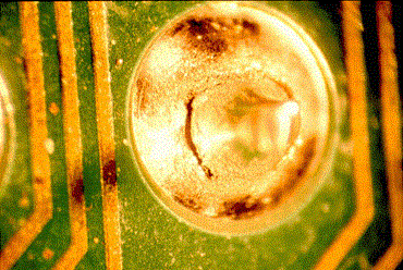
Case Study: Addressing Solder Joint Failures in High-Temperature Applications
In high-temperature environments, such as industrial control systems, solder joint failures often stem from thermal stress and CTE mismatch. Consider a scenario where a power module on a PCB experiences repeated failures during operation. Analysis reveals that the original footprint used rectangular pads with minimal thermal vias, concentrating stress at the joint. By redesigning the footprint to include rounded pads and a grid of thermal vias, stress distribution improved significantly. Post-revision testing under IPC-9701A conditions showed a marked reduction in joint cracking. This example underscores how tailored footprint design, grounded in industry standards, directly boosts PCB reliability.
Conclusion
Enhancing PCB reliability through better footprints is a critical task for electrical engineers aiming to build robust electronic systems. By understanding the interplay of solder joint mechanics, thermal stress, and CTE mismatch, designers can create footprints that withstand operational challenges. Practical strategies, such as aligning pad geometry with component needs, optimizing for thermal management, and validating through standardized testing, provide a clear path to success. Adherence to recognized guidelines like those from IPC and JEDEC ensures designs meet industry expectations for durability. Ultimately, investing time in footprint optimization translates to fewer failures, longer product life, and greater confidence in PCB performance across diverse applications.
FAQs
Q1: How does footprint design impact solder joint reliability?
A1: Footprint design directly affects solder joint reliability by determining how evenly solder is distributed during reflow. Properly sized and shaped pads ensure strong mechanical and electrical connections. Standards like IPC J-STD-001H guide acceptable joint formation. Poor designs lead to voids or weak bonds, increasing failure risks under stress.
Q2: What role does thermal stress play in PCB failures?
A2: Thermal stress, caused by temperature fluctuations, strains solder joints and components. It accelerates fatigue and cracking, especially in poorly designed footprints. Following test protocols from IPC-9701A helps engineers assess and mitigate these risks. Proper pad geometry can distribute stress more effectively.
Q3: How can engineers address CTE mismatch in footprint design?
A3: CTE mismatch occurs when materials expand differently under heat, stressing solder joints. Engineers can use flexible pad designs, like slotted shapes, to absorb strain. Selecting compatible materials and testing per JEDEC JESD22-B106D standards also helps. This approach enhances long-term reliability.
Q4: Why are industry standards important for footprint reliability?
A4: Industry standards from IPC and JEDEC provide proven guidelines for footprint design and testing. They ensure consistency in solder joint quality and thermal performance. Using standards like IPC-7351C for land patterns minimizes errors. Compliance boosts confidence in PCB reliability across applications.
References
IPC J-STD-001H — Requirements for Soldered Electrical and Electronic Assemblies. IPC, 2021.
IPC-7351C — Generic Requirements for Surface Mount Design and Land Pattern Standard. IPC, 2017.
IPC-9701A — Performance Test Methods and Qualification Requirements for Surface Mount Solder Attachments. IPC, 2006.
IPC-A-600K — Acceptability of Printed Boards. IPC, 2020.
JEDEC JESD22-B106D — Resistance to Solder Shock for Through-Hole Mounted Devices. JEDEC, 2016.
JEDEC JEP140 — Guidelines for Characterizing the Thermal Performance of Packaged Electronic Devices. JEDEC, 2002.


