What Exactly Is an Insulated Metal Substrate (IMS) PCB?
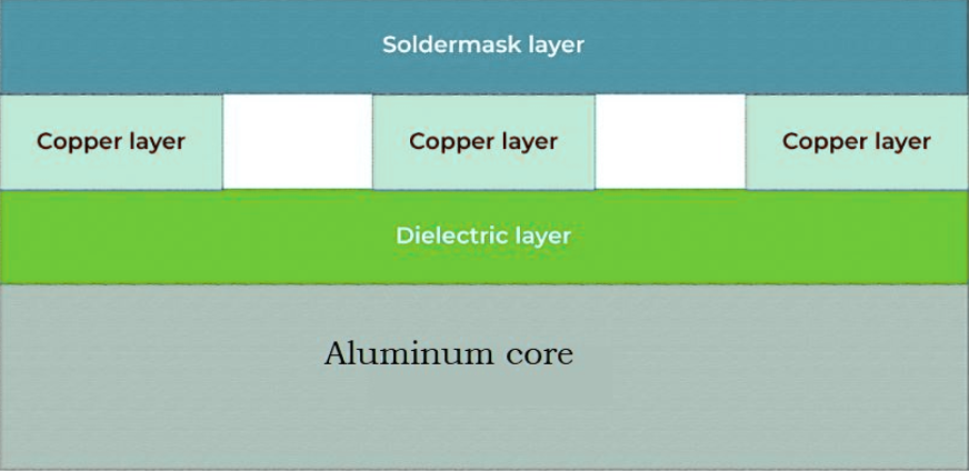
An Insulated Metal Substrate (IMS) PCB, often referred to as a metal core PCB, represents a specialized category of circuit boards engineered for superior heat dissipation. Unlike conventional FR4 boards, an IMS PCB incorporates a metallic base layer, commonly made of aluminum or copper. This metal base is overlaid with a thin dielectric insulating layer, which is then topped with the copper circuitry. This unique layered construction efficiently channels heat away from critical electronic components, making IMS PCBs an ideal choice for applications involving high power levels and significant heat generation.
A fundamental understanding of the IMS PCB's distinctive structure is the cornerstone for effective design. Given that thermal management is central to their purpose, every decision made during the layout phase must prioritize heat dissipation while simultaneously ensuring robust electrical performance and overall product reliability.
Why Is IMS PCB Layout Design So Important?
A meticulously designed IMS PCB layout is critical for achieving efficient heat dissipation, preventing components from overheating, and ultimately extending the operational lifespan of electronic devices. Suboptimal layout choices can lead to localized thermal hotspots, diminished performance, and even premature component failure. By adhering to established IMS PCB layout guidelines and metal core PCB design rules, engineers can circumvent these common pitfalls and develop highly reliable products.
Let's delve into the best practices for designing an IMS PCB layout, with a strong emphasis on thermal management, strategic component placement, and other vital considerations.
Essential IMS PCB Layout Guidelines for Reliability
Designing an IMS PCB necessitates a distinct approach compared to laying out standard FR4 boards. The following are the crucial guidelines to ensure a reliable and efficient design.
Prioritize Thermal Management
The foremost advantage of an IMS PCB lies in its capacity for effective heat dissipation. To fully capitalize on this benefit, your design layout must be centered around thermal management. The metal substrate functions as a heat sink, meaning the primary objective is to transfer heat from the components to this substrate as efficiently as possible.
● Minimize Thermal Resistance: Employ a thin dielectric layer characterized by high thermal conductivity. Dielectric thicknesses typically range from 20 to 100 micrometers, striking a balance between thermal performance and electrical insulation. A thinner layer reduces thermal resistance but must possess adequate dielectric strength (often 500-1000V) to prevent electrical breakdown.
● Select Appropriate Materials: Opt for dielectric materials with enhanced thermal conductivity, such as those filled with ceramic or boron. These materials can achieve thermal conductivity values of 1-3 W/mK, significantly outperforming standard prepreg, which typically offers around 0.3 W/mK.
Related Reading: What Are The Best Thermal PCB Design Practices?
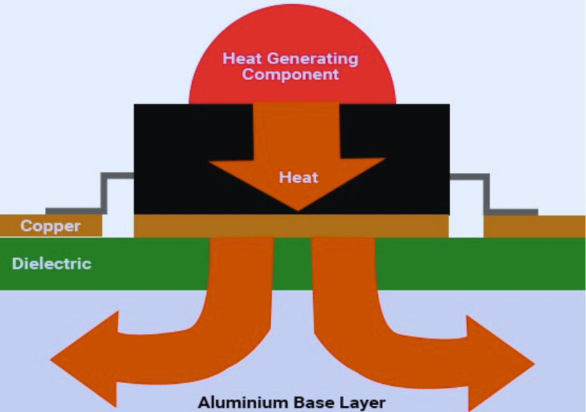
Optimizing Thermal Via Placement
Thermal vias are indispensable for efficiently transferring heat from the top circuitry layer of the PCB to the metal substrate. Strategic thermal via placement in IMS PCB can dramatically improve heat dissipation capabilities.
● Locate Vias Near Heat Sources: Position thermal vias directly underneath or in close proximity to high-power components, such as power transistors or LEDs. This minimizes the distance heat must travel to reach the metal base.
● Utilize Multiple Vias: For components that generate significant heat, a single via is often insufficient. Employ an array of vias (e.g., 4-8 vias per component) to create multiple thermal paths. For instance, a component dissipating 5W might necessitate a combined thermal resistance of less than 10°C/W from its vias.
● Via Size and Spacing: Use vias with a diameter of 0.3-0.5mm for optimal heat transfer. Space them at least 1.5 times the via diameter apart to maintain the structural integrity of the board.
● Consider Via Filling: Filled or plugged vias typically offer superior thermal conductivity compared to open vias. Copper-filled vias, for example, can reduce thermal resistance by as much as 30%.
Related Reading: Thermal Via Placement for Efficient Cooling in 4 Layer PCBs
Strategic Component Placement
Effective component placement for IMS PCB is another critical factor in achieving product reliability. Poor positioning can create localized thermal hotspots or impede the overall heat dissipation process.
● Position High-Power Components Strategically: Place heat-generating components, such as power ICs or resistors, in areas with direct thermal access to the metal substrate or dedicated thermal vias. Avoid clustering multiple high-power components in one area to prevent localized overheating.
● Maximize Spacing: Ensure adequate spacing between components to facilitate even heat dissipation. For example, maintain at least 2-3mm spacing between high-power components to mitigate thermal interference.
● Account for Airflow: If your design incorporates active cooling solutions (e.g., fans), arrange components to take advantage of intended airflow patterns. Place taller components downstream to avoid obstructing cooling for smaller parts.
Suggested Reading: PCB Component Placement: Optimizing for Manufacturing and Assembly
Adhering to Metal Core PCB Design Rules for Electrical Performance
While thermal management is a primary objective, maintaining robust electrical performance is equally important. Adhering to specific metal core PCB design rules ensures signal integrity and prevents unwanted interference.
● Ground Plane Design: Implement a solid ground plane, connecting it to the metal substrate (where feasible) to minimize electromagnetic interference (EMI). Ensure the ground plane remains continuous and uninterrupted, particularly near sensitive analog or high-frequency signal paths.
● Trace Width and Spacing: Calculate trace widths based on both current-carrying capacity and heat dissipation requirements. For high-current traces, use wider tracks (e.g., 0.5-1mm for 5A) to reduce resistive heating. Maintain a minimum spacing of at least 0.2mm between traces to prevent crosstalk.
● Avoiding Sharp Corners: Utilize 45-degree angles or smooth, rounded corners for traces. This helps to reduce signal reflections and minimize stress concentrations, which can be critical for reliability in high-frequency designs.
Additional Insulated Metal Substrate Design Considerations
Beyond thermal and electrical factors, several other insulated metal substrate design considerations contribute to a reliable IMS PCB layout.
● Board Thickness: The metal substrate thickness typically ranges from 0.8mm to 2mm, depending on the application's demands. Thicker substrates (e.g., 1.6mm) offer enhanced heat spreading for high-power designs but will increase the overall weight and cost.
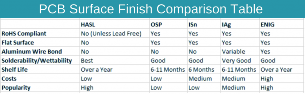
● Surface Finish: Select a surface finish that supports both thermal and electrical performance. Electroless Nickel Immersion Gold (ENIG) is often favored for its exceptional flatness and corrosion resistance, which is crucial for good thermal contact. In contrast, Hot Air Solder Leveling (HASL) can create uneven surfaces that may negatively impact thermal performance.
● Mechanical Stability: IMS PCBs, due to their metal core, are inherently more rigid than FR4 boards. This rigidity should be factored into the enclosure design to prevent undue stress on mounting points or connectors.
Common Challenges in IMS PCB Design and Their Solutions
Designing IMS PCBs presents unique challenges. Here are some frequently encountered issues and practical strategies to overcome them.
Balancing Thermal and Electrical Insulation
The dielectric layer within an IMS PCB must provide effective electrical insulation while simultaneously allowing heat to pass through efficiently. A layer that is too thick will increase thermal resistance, while a layer that is too thin risks electrical breakdown.
Solution: Collaborate with your PCB manufacturer to select a dielectric material with a thermal conductivity of at least 1 W/mK and a dielectric strength of 500V or higher for most applications.
Managing Cost vs. Performance
High-performance materials, such as ceramic-filled dielectrics or copper substrates, can significantly increase manufacturing costs.
Solution: For cost-sensitive projects, consider using aluminum as the metal base (thermal conductivity of ~200 W/mK) instead of copper (~400 W/mK). Aluminum can still provide adequate heat dissipation for many applications, offering a good balance.
Ensuring Manufacturability
IMS PCBs often have specific fabrication requirements due to their metal core. Overly complex designs with an excessive number of vias or very fine traces can be challenging to manufacture.
Solution: Adhere to standard design rules, such as minimum trace widths of 0.15mm and via diameters of 0.3mm, unless your project explicitly demands tighter tolerances. Simplification often leads to higher yields.
Applications of IMS PCBs and Design Tailoring
IMS PCBs are extensively utilized in industries where effective heat management is paramount. Tailoring your design to the specific application can further enhance overall reliability.
● LED Lighting: Focus on precise thermal via placement directly beneath LED chips to manage the significant heat generated by high-brightness LEDs. For larger fixtures dissipating over 10W, consider a thicker metal base (e.g., 1.6mm).
● Automotive Electronics: Prioritize robust ground planes to effectively manage electromagnetic interference (EMI) from adjacent vehicle systems. Ensure components are adequately spaced to withstand vibration and severe thermal cycling.
● Power Supplies: Optimize trace widths for high current (e.g., 1mm for 10A) and position power components near the board edges to facilitate better heat sinking and thermal transfer to external cooling elements.
Final Recommendations for a Reliable IMS PCB Layout
Creating a reliable IMS PCB layout demands meticulous attention to thermal, electrical, and mechanical factors. Here are some concluding tips to keep in mind.
● Simulate your design extensively using thermal analysis software to proactively identify potential hotspots before fabrication. Advanced tools can predict temperature rises (e.g., a 20°C increase under load) and guide optimal via placement.
● Engage in early collaboration with your PCB supplier during the design process to confirm material availability, discuss manufacturability constraints, and ensure smooth production.
● Rigorously test prototypes under real-world operating conditions to validate thermal performance. For instance, accurately measure the junction temperatures of critical components to ensure they remain below their specified maximum (e.g., 125°C) for long-term reliability.
Conclusion
Developing a reliable IMS PCB layout is fundamentally about striking a precise balance between thermal management, electrical performance, and manufacturability. By consistently applying these IMS PCB layout guidelines and metal core PCB design rules, you can effectively optimize thermal via placement, enhance component positioning, and meticulously address all critical insulated metal substrate design considerations. Whether your project involves LED lighting, automotive systems, or power electronics, a well-designed IMS PCB will significantly boost the performance and extend the lifespan of your product.
At AIVON, we are dedicated to empowering engineers with the essential tools and resources needed to transform innovative designs into reality. With these best practices in hand, you are now equipped to confidently approach your next IMS PCB project.


