Why Are Differential Pairs Essential in High-Speed PCB Design?
In the rapidly evolving landscape of modern electronics, high-speed printed circuit board (PCB) designs are crucial for ensuring reliable data transmission across various applications, including USB, HDMI, Ethernet, and PCIe. A core technique within these designs is differential pair routing, which significantly enhances signal integrity, minimizes electromagnetic noise, and effectively supports high-speed communication. For engineers, gaining expertise in differential pair routing is fundamental to developing robust and efficient PCBs that meet demanding performance specifications.
This article delves into the foundational principles, practical techniques, and recommended best practices for differential pair routing in high-speed PCB layouts. Whether you are working on a compact IoT device or a complex data center system, these insights will help you optimize your designs for superior signal integrity and performance.
What Are Differential Pairs and What Makes Them Critical?
Differential pairs are composed of two traces that carry electrical signals of equal magnitude but opposite polarity, typically referenced to a common ground plane. Unlike single-ended signaling, which relies on a single trace and a ground plane for the return path, differential signaling transmits data by utilizing the voltage difference between the two traces. This method offers several distinct advantages:
Key Advantages of Differential Pairs
● Enhanced Noise Immunity: Common-mode noise, such as electromagnetic interference (EMI), affects both traces equally, allowing it to be effectively canceled out at the receiving end.
● Superior Signal Integrity: Differential pairs maintain signal quality over extended distances, making them ideal for high-speed interfaces where signal degradation must be minimized.
● Support for Higher Data Rates: Protocols like USB (which uses 90 ohms impedance) and PCIe (85 ohms) rely on differential pairs to achieve reliable, high-speed data transfer.
Differential pairs are integral to many high-speed interfaces, including USB 3.0 (5 Gbps), HDMI 2.0 (6 Gbps per channel), and Ethernet (10 Gbps). However, to fully realize these benefits, strict routing requirements must be met to maintain symmetry, controlled impedance, and precise signal timing.F
What Are the Core Principles for Routing Differential Pairs?
To achieve optimal performance, differential pair routing must adhere to several fundamental principles. These guidelines ensure signal synchronization, controlled impedance, and minimal noise interference.
Essential Routing Principles
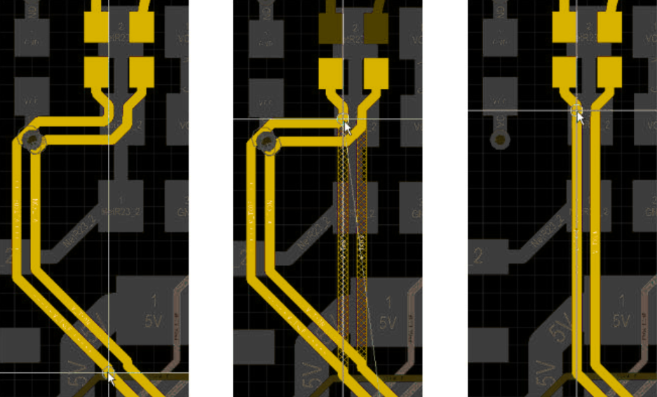
1. Maintaining Trace Symmetry: Symmetry between the two traces is paramount. Both traces must possess identical lengths, widths, and spacing to ensure that their respective signals arrive at the receiver simultaneously. Even minor mismatches can introduce skew, leading to timing errors. For example, a mere 1 mm length difference in a 10 Gbps signal can result in approximately 6.7 picoseconds of delay, potentially violating critical timing margins.
2. Controlling Impedance: Differential pairs require a specific differential impedance, which is typically defined by the signaling standard (e.g., 90 ohms for USB, 100 ohms for Ethernet). This impedance is significantly influenced by trace width, the spacing between traces, and the dielectric properties of the PCB material. Maintaining consistent impedance along the entire length of the traces is essential to prevent signal reflections and subsequent signal degradation.
3. Minimizing Crosstalk: Crosstalk occurs when signals from adjacent traces interfere with the differential pair. To reduce crosstalk, it is vital to maintain a clearance of at least three times the trace width between differential pairs and other traces. For particularly high-speed signals, broadside routing on adjacent layers can be considered to increase routing density while effectively managing crosstalk.
4. Optimizing Return Paths: A robust and continuous ground plane situated directly beneath the differential pair provides a low-impedance return path, which reduces EMI and preserves signal integrity. It is critical to avoid routing differential pairs over split planes, as this disrupts the return path and can create a "loop antenna" effect, significantly increasing noise.
What Are Best Practices for Implementing Differential Pair Routing?
Drawing from industry standards and insights from leading PCB design experts, here are actionable best practices to guide your differential pair routing for enhanced performance.
Routing Traces Closely and Matching Lengths
1. Route Traces in Close Proximity: Keep the two traces of a differential pair as close as possible throughout their entire path. Tight coupling (e.g., spacing of 5-10 mils for a 5-mil trace width) ensures that both traces experience similar electrical conditions, thereby minimizing noise and signal distortion. Utilize PCB design software, such as Cadence or Altium, to define and enforce differential pair constraints, guaranteeing consistent spacing and width.
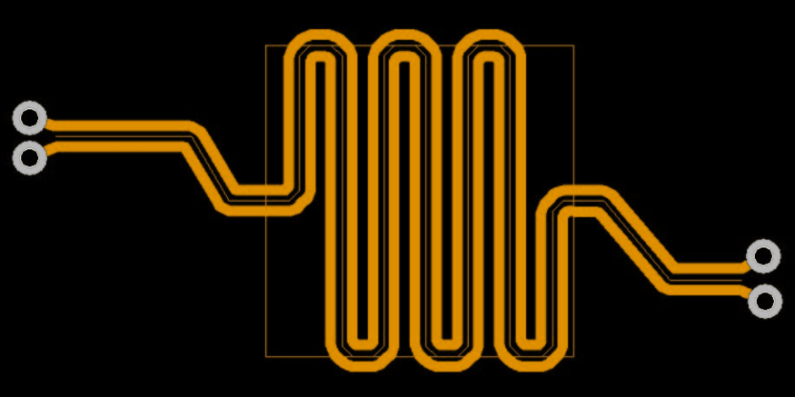
2. Ensure Matched Trace Lengths: Length matching is critical to prevent skew. For high-speed interfaces such as PCIe, the length tolerance within a pair is typically very tight, often ±5 mils. Serpentine routing (also known as trombone routing) can be used to extend the shorter trace, but ensure the geometry is carefully designed with smooth 135° angles for bends to minimize impedance discontinuities and reduce EMI.
Minimizing Vias and Maintaining Layer Consistency
1. Minimize and Symmetrize Vias: Vias can introduce impedance discontinuities and lead to signal degradation. If vias are unavoidable, place them symmetrically for both traces within the pair, and ensure the same number of vias is used for each trace. For example, when transitioning a differential pair from the top layer to an inner layer in a 4-layer PCB, two vias (one per trace) should be placed equidistant from the pads. Consider back-drilling vias to reduce stub lengths and further minimize reflections.
2. Route on a Single Layer: Routing both traces of a differential pair on the same layer ensures consistent impedance and signal propagation speed. Signal propagation characteristics can vary between layers due to differences in dielectric constants (e.g., FR-4 typically has a dielectric constant of ~4.2). If layer transitions are absolutely necessary, use stitching capacitors to maintain a continuous return path across reference planes.
Utilizing a Solid Ground Plane and Symmetric Capacitor Placement
1. Utilize a Solid Ground Plane: A continuous ground plane beneath the differential pair is essential for minimizing EMI and providing a stable reference voltage. For a 4-layer PCB, dedicate one inner layer entirely to a ground plane. Avoid routing traces over split ground planes, as this disrupts the return path and increases noise coupling. If a split plane cannot be avoided, route the traces carefully around it or use stitching capacitors to bridge the gap.
2. Symmetrical Placement of Coupling Capacitors: Some high-speed differential pairs, such as those found in PCIe, require serial coupling capacitors. Use smaller package sizes (e.g., 0402 instead of 0603) to minimize impedance discontinuities, and place these capacitors symmetrically to preserve precise signal timing. For example, a 0.1 µF capacitor placed 50 mils from the transmitter can help ensure balanced signal propagation.
What Are Common Challenges in Differential Pair Routing and Their Solutions?
Differential pair routing often presents several challenges, particularly in high-density or ultra-high-speed designs. Here are common issues and effective strategies to address them.
Overcoming Routing Difficulties
1. Crosstalk from Adjacent Traces:
a. Challenge: Adjacent single-ended traces or other differential pairs can induce crosstalk, leading to degradation of signal quality.
b. Solution: Increase the spacing to at least three times the trace width (e.g., 15 mils for a 5-mil trace). Additionally, use guard traces that are grounded with vias at regular intervals (e.g., every 500 mils) to provide shielding for sensitive differential pairs.
2. Impedance Mismatches:
a. Challenge: Inconsistencies in trace width, spacing, or dielectric thickness can cause impedance mismatches, resulting in undesirable signal reflections.
b. Solution: Employ a field solver within your PCB design software to accurately calculate the trace geometry required for the target impedance (e.g., 100 ohms for Ethernet). Verify the planned PCB stackup with your manufacturer to ensure consistent dielectric properties.
3. Skew Due to Asymmetric Routing:
a. Challenge: Asymmetrical routing patterns around components or vias can introduce skew, disrupting critical signal timing.
b. Solution: Implement symmetric fan-out patterns at both the driver and receiver ends. For instance, when routing from a fine-pitch BGA, ensure that the track lengths to the fan-out vias are equal, as per industry best practices.
4. Manufacturing Limitations:
a. Challenge: Very tight trace spacing or extremely small via sizes might exceed standard manufacturing capabilities, potentially increasing PCB cost or leading to defects.
b. Solution: Engage with your PCB manufacturer early in the design phase to confirm their minimum trace width (e.g., 4 mils) and spacing (e.g., 4 mils) capabilities. Adjust your design rules accordingly to strike a balance between desired performance and manufacturability.
What Advanced Techniques Improve High-Speed Designs?
For cutting-edge applications, such as 5G infrastructure or advanced data center equipment, consider these advanced techniques to push the boundaries of performance.
Cutting-Edge Routing Methods
1. Broadside Differential Pairs: Route differential pairs on adjacent signal layers in a broadside configuration to increase routing density and reduce crosstalk. This approach demands a highly precise stackup design to maintain consistent impedance, as the dielectric thickness between layers directly impacts coupling.
2. Zigzag Routing for Fiber Weave Mitigation: To mitigate the effects of fiber weave in extremely high-speed designs, route traces at a slight angle (e.g., 15°) on alternating layers. This technique helps reduce crosstalk and improves overall signal integrity, particularly for dual stripline configurations.
3. Comprehensive Signal Integrity Simulation: Before commencing fabrication, utilize advanced simulation tools, such as Altium Designer's signal integrity analyzer, to accurately predict the behavior of differential pairs. Simulate impedance, crosstalk, and propagation delay to identify and resolve potential issues early in the design cycle, thereby saving valuable time and reducing costs.
How AIVON Supports Your High-Speed PCB Design Needs
At AIVON, we fully comprehend the intricate complexities of high-speed PCB design and differential pair routing. Our advanced manufacturing capabilities and rapid PCB prototyping services are designed to empower engineers to confidently bring their sophisticated designs to fruition. With extensive global logistics and state-of-the-art facilities, we guarantee the precise fabrication of high-speed PCBs, meeting rigorous tolerances for trace width, spacing, and impedance control. Whether you are prototyping a 5G module or scaling up production for IoT devices, AIVON’s specialized expertise and rapid delivery systems help you achieve reliable, high-performance results.
Conclusion: The Future of High-Speed PCB Design with Differential Pairs
Differential pair routing stands as a cornerstone of high-speed PCB design, enabling robust and reliable signal transmission in today’s sophisticated electronic systems. By diligently adhering to fundamental principles such as trace symmetry, controlled impedance, and establishing proper return paths, engineers can effectively minimize noise and guarantee optimal signal integrity. Best practices, including meticulous length matching, minimal via usage, and the provision of solid ground planes, further enhance performance. Meanwhile, advanced techniques like broadside routing and sophisticated signal simulation address the rigorous demands of cutting-edge applications.
Suggested Reading: Differential Pair Routing: Best Practices for High Speed Signal Transmission
By systematically applying these techniques and effectively leveraging modern PCB design tools, you can create layouts that consistently meet the stringent requirements of high-speed interfaces. AIVON is dedicated to supporting your journey with high-quality manufacturing and prototyping services meticulously tailored to your specific, high-performance results.