Introduction
In high-speed PCB design, ground plane partitioning emerges as a critical strategy for preserving PCB signal integrity. Engineers face increasing challenges from signal speeds exceeding gigahertz frequencies, where noise coupling and return path disruptions can degrade performance. Ground plane partitioning signal integrity directly addresses these issues by isolating sensitive analog sections from noisy digital domains. This approach optimizes return paths, maintains controlled impedance, and minimizes electromagnetic interference. As data rates climb, mastering this technique becomes essential for reliable operation in telecommunications, computing, and automotive electronics. Proper implementation ensures clean signal transmission while adhering to established design principles.
What Is Ground Plane Partitioning?
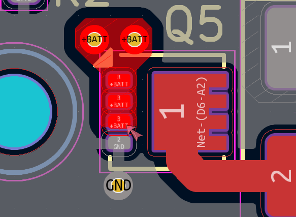
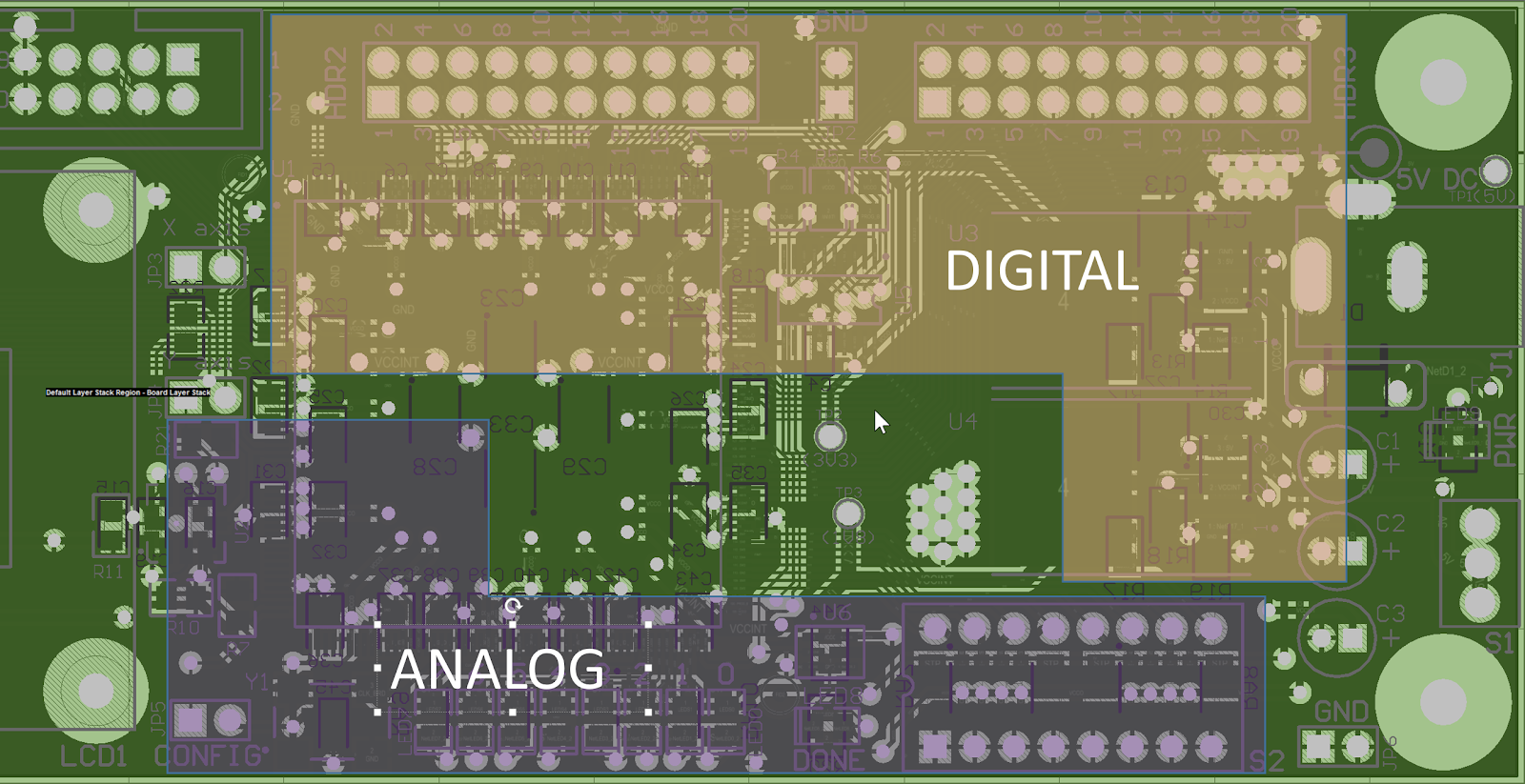
Ground plane partitioning involves dividing a continuous ground plane into distinct sections on the same layer, typically to separate analog, digital, or power domains. This technique creates physical barriers, such as slits or moats, that prevent unwanted current flows between sections. In multilayer boards, partitioning applies to inner ground layers adjacent to signal traces. The goal centers on return path optimization, ensuring high-frequency return currents follow predictable paths close to their outgoing signals. Without partitioning, shared grounds allow digital switching noise to corrupt analog signals through common impedance coupling. Engineers apply this method selectively in mixed-signal designs to balance isolation and continuity.
Partitioning differs from full plane splits, which remove connectivity entirely; instead, it maintains overall integrity via strategic bridges. These bridges, often implemented with zero-ohm resistors or capacitors, provide DC connections while filtering high-frequency noise. The process requires careful planning during stackup definition and routing stages. Signal traces must respect partition boundaries to avoid crossing gaps without support. This structured separation enhances overall PCB signal integrity by localizing noise sources.
Related Reading: PCB Ground Planes – What are They and Why are They Important?
Why Ground Plane Partitioning Matters for Signal Integrity
Ground plane partitioning signal integrity proves vital in environments with mixed signal types, where digital transients can induce voltage fluctuations on analog grounds. High-speed signals demand low-impedance return paths; unpartitioned planes force return currents to detour, increasing loop inductance and radiated emissions. This leads to crosstalk between adjacent traces and ground bounce during simultaneous switching. In high-speed PCB design, such disruptions distort eye diagrams, elevate bit error rates, and violate timing margins. Partitioning confines return currents to dedicated zones, preserving impedance control in PCBs and reducing EMI susceptibility.
Beyond noise isolation, partitioning supports thermal management by directing heat from power-hungry sections away from precision circuits. Compliance with IPC-2221 guidelines reinforces these benefits, emphasizing plane usage for stable reference potentials. Engineers observe measurable improvements in signal-to-noise ratios post-partitioning, particularly above 500 MHz. Neglecting this practice risks product failures in field deployments, underscoring its relevance for robust designs.
Technical Principles Behind Ground Plane Partitioning
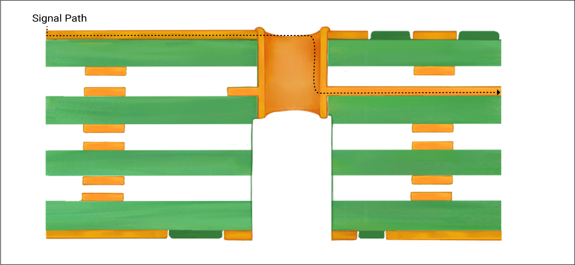
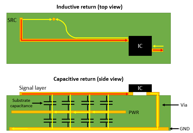
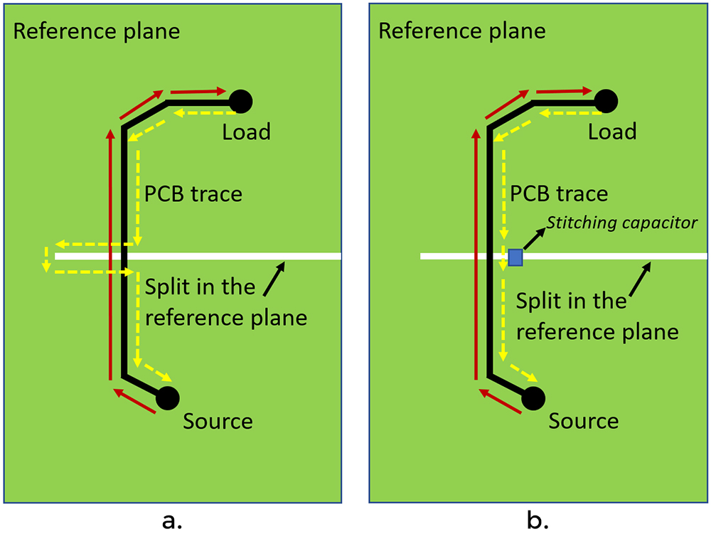
At high frequencies, return currents concentrate beneath signal traces due to skin effect and proximity principles, forming an image plane effect. A continuous ground plane provides the ideal low-inductance return, but shared usage couples noise across domains. Partitioning exploits domain isolation by aligning trace return paths strictly within their sections, minimizing inductive loops. Gaps wider than trace width disrupt this flow, creating high-impedance discontinuities that reflect signals and amplify ringing. Stitching vias along partition edges restore continuity for low-frequency returns while blocking high-frequency propagation.
Impedance control in PCBs relies on uniform reference planes; partitioning introduces variations if not managed. Engineers calculate gap widths based on frequency, ensuring they exceed one-tenth wavelength to avoid coupling. Capacitive coupling across slits must stay below -40 dB for sensitive applications. Multi-layer stackups amplify these effects, as inner planes handle most returns. Understanding these mechanisms allows precise partitioning without compromising overall integrity.
Ground bounce arises from simultaneous switching on unpartitioned planes, elevating ground potential and modulating signals. Partitioning localizes this bounce, protecting distant traces. Ferrite beads or inductors at bridges filter residual noise, combining inductive and resistive damping.
Best Practices for Ground Plane Partitioning in High-Speed Designs
Begin partitioning during schematic capture by assigning unique ground nets for domains, then translate to layout with clearance rules. Position partitions parallel to signal flow, avoiding perpendicular crossings that lengthen return detours. For traces bridging sections, route them over bridges with paired vias immediately before and after the gap, minimizing stub inductance. Maintain gap widths at least three times the trace-to-plane spacing to suppress fringing fields. Use simulation tools to verify pre-layout return path integrity through S-parameter analysis.
Stitching vias, spaced at one-eighth wavelength intervals, bridge partitions for broadband returns. Place decoupling capacitors across bridges, sized for dominant frequencies, to shunt high-frequency currents. In four-layer boards, dedicate inner layers to partitioned grounds adjacent to signals. Adhere to IPC-2221 recommendations for plane widths and spacing to ensure mechanical stability. Verify post-layout with field solver extractions for impedance profiles.
Related Reading: Power and Ground Plane Design in 4 Layer PCBs
Optimize stackup by sandwiching signals between dedicated planes, reducing enclosure resonance. For high-speed PCB design, prioritize solid copper fills over hatched planes to lower resistance. Route power over separate planes to decouple from grounds further. Final DRC checks flag violations like traces over gaps without vias.
Common Pitfalls and Troubleshooting in Partitioning
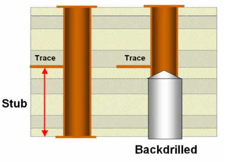
A frequent error involves signals crossing partitions without via pairs, injecting inductance spikes up to several nanohenries. This manifests as overshoot and jitter in time-domain reflectometry. Solution: reroute traces or add redundant vias. Another pitfall is insufficient stitching density, allowing EMI leakage; increase via count and simulate coupling.
Ground loops form if multiple bridges create parallel paths, circulating currents at 50/60 Hz. Single-point star grounding resolves this, often at board entry. Thermal vias near power sections prevent hotspots from warping partitions. Troubleshooting starts with scope probing for noise spectra, followed by spectrum analysis to pinpoint sources.
In multilayer boards, misalignment during fabrication exacerbates issues; specify tolerances per IPC-6012 performance specs. Iterative prototyping with boundary scan testing confirms fixes.
Conclusion
Ground plane partitioning signal integrity stands as a cornerstone of advanced PCB design, enabling return path optimization amid rising speeds. By isolating domains, engineers achieve superior impedance control in PCBs, curtailing noise and EMI. Key practices like strategic stitching, via pairing, and simulation ensure success. While challenges exist, adherence to principles yields reliable high-speed performance. Integrating these techniques elevates designs from functional to exceptional.
FAQs
Q1: When should engineers use ground plane partitioning for PCB signal integrity?
A1: Ground plane partitioning signal integrity suits mixed-signal boards where digital noise threatens analog precision, such as ADCs or RF front-ends. Avoid it in pure digital high-speed designs favoring continuous planes for unbroken returns. Assess via noise budget analysis; partition if coupling exceeds 1% of signal amplitude. Follow layout rules to place noisy ICs away from sensitive areas.
Q2: How does partitioning affect return path optimization in high-speed PCB design?
A2: Partitioning confines return currents to local paths, reducing loop areas and inductance compared to detours on shared planes. Bridges with capacitors maintain low-frequency unity while isolating harmonics. Simulations confirm path impedance stays below 50 ohms. Proper execution enhances eye opening by 20-30% in multi-Gbps links.
Q3: What role do stitching vias play in impedance control in PCBs with partitions?
A3: Stitching vias provide low-impedance shunts across gaps, ensuring continuous reference for returns at all frequencies. Space them at lambda/8 for the highest edge rate to minimize discontinuities. Combine with decoupling for PDN stability. This practice aligns with design standards, preventing reflections that degrade signals.
Q4: Can ground plane partitioning increase EMI in high-speed designs?
A4: Yes, if gaps create radiating slots, but mitigation via stitching and shielding suppresses this. Route crossings perpendicular to edges and verify with near-field scans. Continuous planes often outperform in pure digital, but partitioning excels in mixed environments with proper implementation.
References
IPC-2221A — Generic Standard on Printed Board Design. IPC
IPC-6012E — Qualification and Performance Specification for Rigid Printed Boards. IPC, 2017
IPC-A-600K — Acceptability of Printed Boards. IPC, 2020