Introduction
Handling irregular shaped printed circuit boards presents unique challenges in high-volume manufacturing. Electrical engineers often encounter designs with non-rectangular outlines due to space constraints in enclosures or specific mechanical requirements. Tab routing emerges as a critical technique in PCB panelization for these complex geometries. This method secures multiple boards within a larger panel using breakaway tabs, enabling efficient fabrication and assembly processes. By mastering tab routing PCB panelization, engineers can minimize handling damage and optimize throughput. This article explores the principles, best practices, and considerations for effective implementation.
What Is Tab Routing and Why It Matters in PCB Panelization
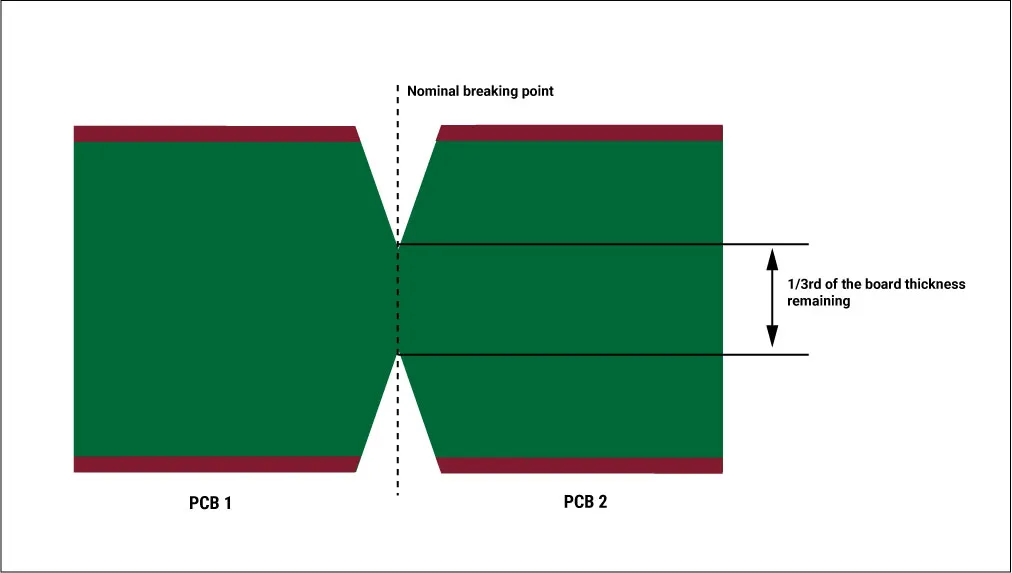
Tab routing involves milling the outline of individual PCBs within a panel, leaving strategically placed tabs to hold the boards together during processing. These tabs, often perforated with mouse bites, allow clean separation post-assembly without compromising board integrity. Unlike V-scoring, which suits rectangular boards, tab routing accommodates irregular shapes where straight-line scoring proves impractical. In PCB mouse bites design, perforations weaken the tabs precisely, facilitating manual or automated depaneling.
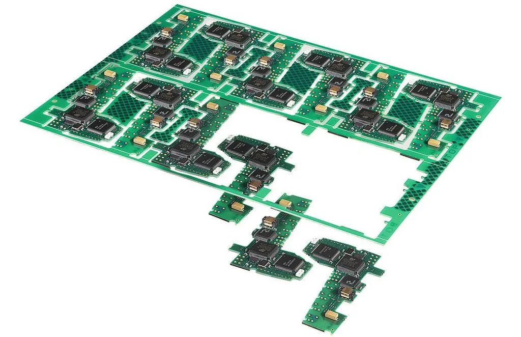
The relevance of tab routing PCB panelization lies in its versatility for diverse applications. Irregular PCBs, common in consumer electronics and automotive modules, benefit from reduced material waste and streamlined pick-and-place operations. Proper panelization enhances yield by distributing mechanical stresses evenly across the array. Engineers prioritizing breakaway tab design guidelines ensure compliance with fabrication tolerances, avoiding issues like delamination. Ultimately, this approach supports scalable production while maintaining structural stability through reflow and testing stages.
Technical Principles of Tab Routing for Irregular PCBs
The core mechanism of tab routing relies on controlled material removal around board perimeters, preserving tabs as mechanical anchors. These tabs distribute forces during handling, preventing panel warpage that could misalign fiducials or components. Perforations in tabs, known as mouse bites, create a predictable fracture line by reducing cross-sectional strength at intervals. This design principle minimizes propagation of cracks into functional areas during depaneling irregular PCBs.
Stress analysis plays a key role in tab routing efficacy. Forces applied during separation concentrate at tab roots, necessitating rounded geometries to avoid sharp stress risers. Material properties, such as FR-4 rigidity, influence tab resilience under thermal cycling. Adhering to IPC-6012E qualification specifications for rigid printed boards ensures panels withstand fabrication stresses without defects. Engineers must consider panel thickness uniformity to maintain consistent routing depths across irregular outlines.
Depaneling mechanics further underscore tab routing's advantages. Manual snapping leverages the weakened perforations for low-force separation, while routing tools follow precise paths for high-volume runs. Vibration and shock during detachment can induce microcracks if tabs are poorly placed. Thus, positioning tabs along non-critical edges preserves trace integrity and solder joint reliability.
Breakaway Tab Design Guidelines and Component Placement
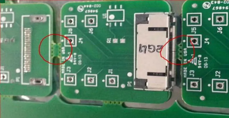
Effective breakaway tab design guidelines emphasize strategic placement and quantity to balance panel stability and ease of separation. Tabs should span sufficient lengths to support board weight without sagging, particularly for thinner substrates. Distributing tabs evenly around irregular perimeters counters asymmetric loads during conveyor transport. Incorporating perforations aligns with standard patterns that promote uniform fracturing, reducing burrs or fiber pullout.
Component placement tab routing requires careful zoning to shield sensitive features from depaneling stresses. Maintain adequate clearances between tabs and nearby elements like capacitors or connectors to prevent mechanical interference. High-density areas demand tabs positioned on opposite sides, avoiding overlap with edge-mounted parts. This layout preserves assembly tolerances and facilitates inspection per IPC-A-600K acceptability criteria for printed boards.
Panel array configuration amplifies these guidelines. Orient identical irregular boards to maximize nesting efficiency, minimizing scrap. Fiducial marks outside tab zones aid alignment for automated processes. Engineers should simulate stress via finite element analysis to validate designs before fabrication.
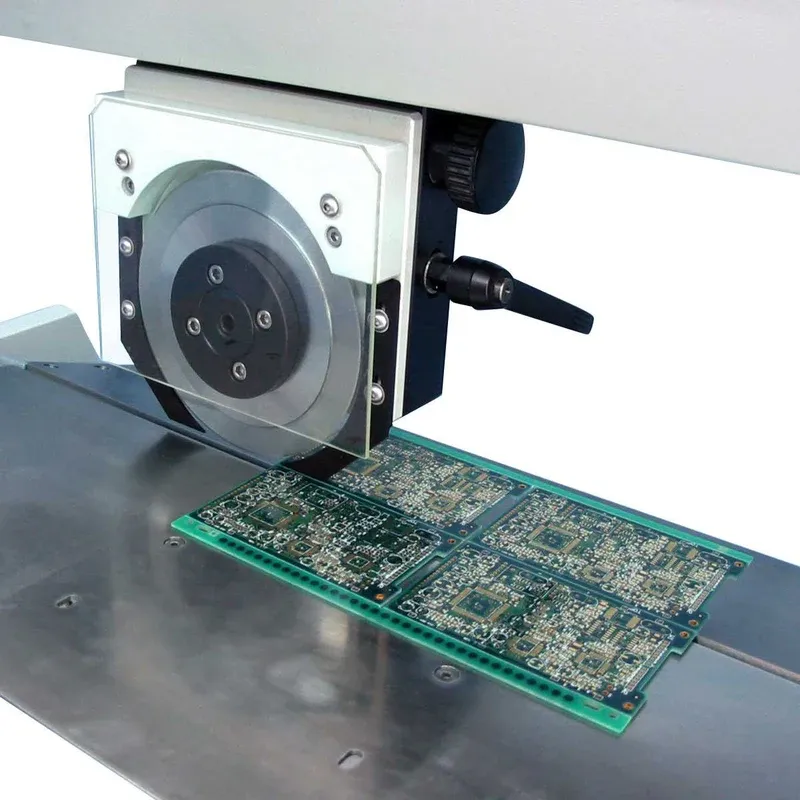
Best Practices for Depaneling Irregular PCBs
Depaneling irregular PCBs via tab routing demands methodical approaches to preserve functionality. Pre-separation inspection verifies tab integrity, identifying any routing anomalies from fabrication. For manual processes, apply force perpendicular to the perforation line, using fixtures to immobilize the panel. Automated routers with spindle control follow programmed paths, extracting tabs cleanly without board contact.
Optimize tab routing by selecting perforation densities suited to board thickness and material. Fewer holes suit robust panels, while denser patterns ease detachment for fragile designs. Post-depaneling, edge finishing removes residues, ensuring compatibility with conformal coating. These practices align with IPC-2221 generic requirements for printed board design, promoting reliability.
Integrate quality checks throughout. Ultrasonic cleaning post-depaneling mitigates contamination from fibers. Electrical testing confirms no latent damage from stresses. Documenting panel yields informs iterative improvements in future layouts.
Troubleshooting Common Challenges in Tab Routing Panelization
Engineers frequently face warpage in tab-routed panels due to uneven copper distribution or thermal mismatches. Symmetrical tab placement mitigates this by equalizing support points. Excessive tab strength leads to tearing rather than clean breaks; refine perforations accordingly. Component shifts during reflow signal inadequate clearances, prompting redesigns with buffered zones.
Burr formation at tab roots arises from dull tooling; specify sharp carbide bits in panel specs. Irregular shapes amplify handling risks, so incorporate edge rails for stability. Analyzing failures through cross-sections reveals root causes, guiding refinements. Consistent application of standards like IPC-6012E elevates troubleshooting outcomes.
Conclusion
Tab routing stands as an indispensable technique for mastering irregular PCB panel designs, offering flexibility where traditional methods falter. By adhering to breakaway tab design guidelines and optimizing component placement tab routing, engineers achieve robust panels with high yields. Key principles include stress management, precise perforations, and strategic layouts. Implementing these practices ensures seamless transitions from fabrication to assembly. Electrical engineers equipped with this knowledge drive efficient, reliable production workflows.
FAQs
Q1: What are the main advantages of tab routing PCB panelization for irregular shapes?
A1: Tab routing excels in accommodating non-rectangular outlines, reducing stress concentrations compared to V-scoring. It supports efficient array layouts with mouse bites for easy depaneling irregular PCBs. This method minimizes material waste and enhances handling stability during SMT processes. Overall, it boosts throughput for complex designs without compromising integrity.
Q2: How does PCB mouse bites design influence breakaway tab performance?
A2: PCB mouse bites design incorporates perforations that weaken tabs predictably, enabling controlled fracturing during separation. Optimal patterns distribute forces evenly, preventing cracks from extending into board areas. This aligns with guidelines for clean edges post-depaneling. Engineers adjust bite density based on panel thickness for reliable results.
Q3: What component placement tab routing rules should engineers follow?
A3: Maintain sufficient distances between tabs and components to avoid damage during depaneling. Position tabs away from high-density zones and edge parts. This preserves solder joints and traces under mechanical stress. Fiducials outside tabs ensure alignment accuracy. Following these enhances assembly yield.
Q4: Why prioritize breakaway tab design guidelines in depaneling irregular PCBs?
A4: Breakaway tab design guidelines ensure even stress distribution and clean separation, critical for irregular shapes. Proper placement and perforations reduce risks like delamination or warpage. They facilitate both manual and automated processes efficiently. Adherence supports standard compliance and production scalability.
References
IPC-6012E — Qualification and Performance Specification for Rigid Printed Boards. IPC, 2017
IPC-A-600K — Acceptability of Printed Boards. IPC, 2020
IPC-2221B — Generic Standard on Printed Board Design. IPC, 2012