Introduction
High-density interconnect (HDI) printed circuit boards represent a critical advancement in electronics, enabling compact designs for smartphones, wearables, and medical devices. Microvias play a central role in HDI technology by providing precise interconnections between layers, far surpassing the capabilities of traditional through-hole vias. These small vias allow for denser routing, reduced signal path lengths, and improved electrical performance in space-constrained applications. Engineers designing HDI PCBs must master microvia design rules, microvia reliability, stacked microvias, laser drilling microvias, and microvia impedance control to achieve optimal results. This guide delivers structured insights into these elements, drawing on established engineering principles to support reliable fabrication and performance.
What Are Microvias and Why Do They Matter in HDI PCB Design?
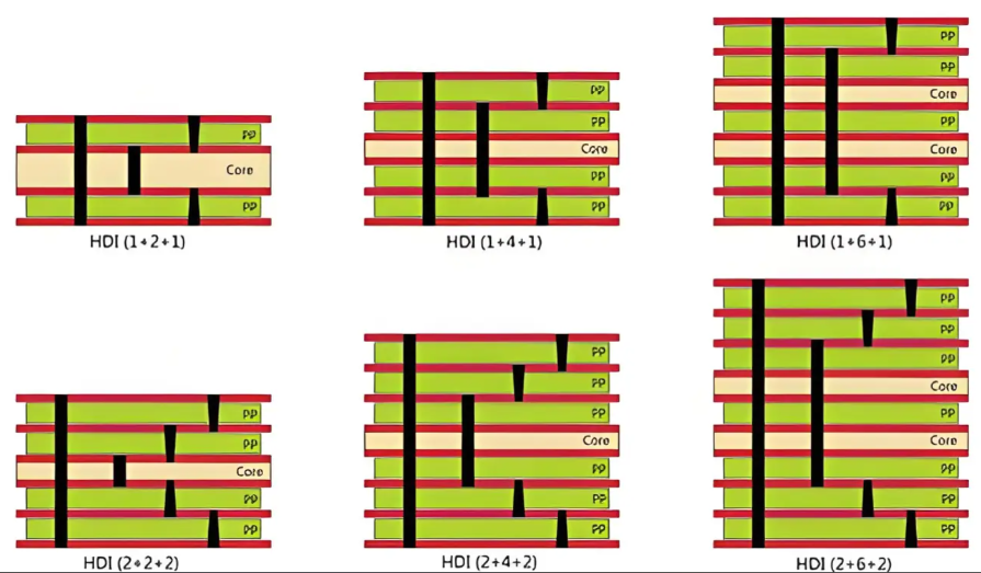
Microvias are blind or buried vias with a laser-drilled diameter of 150 micrometers or less, distinguishing them from standard vias used in conventional PCBs. According to industry definitions, they feature a maximum aspect ratio of 1:1 and a total depth not exceeding 0.25 mm, ensuring manufacturability and plating uniformity. In HDI PCBs, microvias enable sequential build-up processes, where thin dielectric layers are added around a core, supporting structures classified as Type I through Type VI. Their small size minimizes board real estate, allowing finer trace widths and pitches essential for high-pin-count components like BGAs.
The relevance of microvias stems from the demand for miniaturization in modern electronics. They reduce via stubs that cause signal reflections, shorten interconnect lengths to lower latency, and facilitate higher layer counts without excessive thickness. Without microvias, achieving the wiring density required for 5G modules or AI processors would be impractical. Engineers benefit from their use in managing thermal expansion mismatches and enhancing overall board reliability.
Related Reading: Microvia Stackup: The Complete Beginner's Guide
Microvia Design Rules: Essential Parameters for Success
Microvia design rules form the foundation of robust HDI layouts, specifying parameters like diameter, aspect ratio, pad size, and spacing to prevent fabrication defects. A preferred aspect ratio of 0.75:1 ensures complete copper plating at the via bottom, while a maximum of 1:1 maintains reliability under thermal stress. Pad diameters typically range from 100 to 150 micrometers larger than the via hole to provide adequate annular rings, with minimum clearances between microvias set at three times the via diameter to avoid shorts. These rules align with IPC-2226A guidelines, which categorize HDI structures and define density multipliers for routing efficiency.
Land sizes and anti-pad clearances must account for laser beam divergence and registration tolerances during sequential lamination. For instance, outer layer microvias require larger capture pads to compensate for drill smear removal via desmear processes. Engineers should simulate stackups early to verify compliance, as violations can lead to open circuits or weak joints. Adhering to these microvia design rules minimizes yield losses and supports high-volume production.
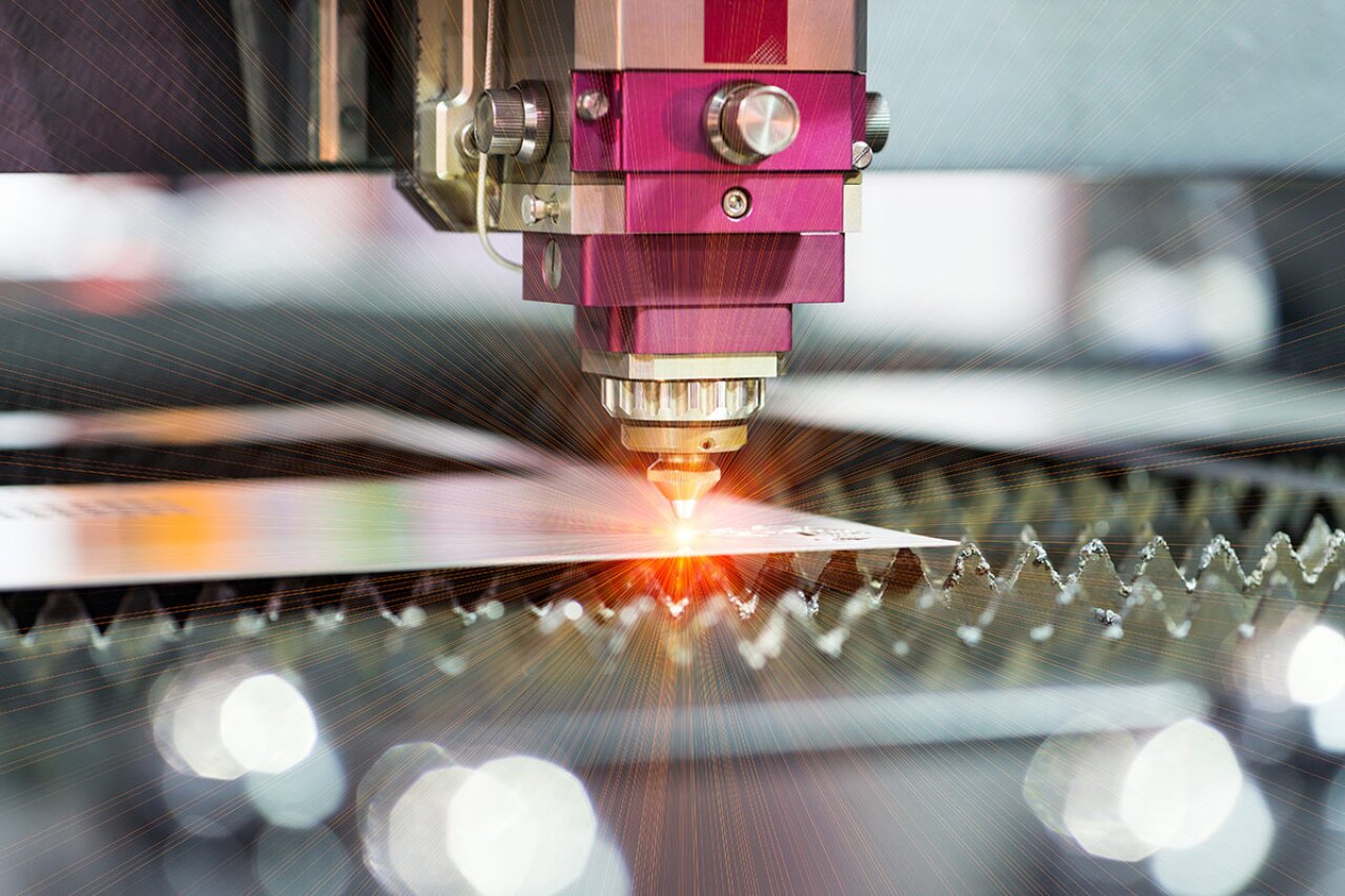
Laser Drilling Microvias: Process Fundamentals and Optimization
Laser drilling microvias involves using CO2 or UV lasers to ablate dielectric materials precisely, creating holes unattainable by mechanical methods. CO2 lasers excel at removing epoxy resins through thermal vaporization, while UV lasers handle glass-reinforced dielectrics with photochemical ablation for cleaner sidewalls. The process occurs in multiple cycles during HDI build-up, with each layer drilled, plated, and laminated sequentially. Parameters like pulse energy, repetition rate, and beam focus control hole taper and heat-affected zones, critical for subsequent plating.
Post-drilling, plasma desmear cleans residues, followed by electroless copper seed and electroplating to fill or plate the barrel. Optimal drill sizes range from 50 to 100 micrometers, balancing density with plating reliability. Engineers optimize by selecting laser-drillable dielectrics with low Tg variation and uniform filler distribution. This approach ensures microvia integrity across HDI layers.
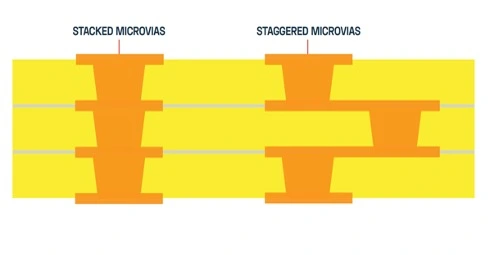
Stacked Microvias vs. Staggered Microvias: Configurations and Trade-offs
Stacked microvias align directly atop one another, connecting multiple layers in a vertical column, ideal for maximal density in any-layer HDI (Type III/IV). However, this configuration concentrates mechanical stress during thermal cycling, potentially leading to microcracks at interfaces. Staggered microvias offset each via, distributing loads and improving microvia reliability, especially beyond two layers. IPC-2226A recommends staggered setups for three or more microvia levels to enhance fatigue resistance.
Choosing between them depends on layer count and performance needs. Stacked vias suit compact designs with filled or plated vias for strength, while staggered reduce plating challenges and support finer pitches. Fabrication costs rise with stacking due to tighter tolerances, but both enable escape routing under fine-pitch BGAs. Engineers model stress via FEA to predict failure modes.
- Stacked Microvias: Density = High; Reliability = Moderate (stress concentration); Typical Use = 2-layer transitions, filled vias
- Staggered Microvias: Density = Medium-High; Reliability = High (load distribution); Typical Use = More than 2 layers, any-layer HDI
Related Reading: Stacked Microvias: Enabling High Density Interconnects for Advanced Electronics
Microvia Reliability: Critical Factors and Testing Strategies
Microvia reliability hinges on plating quality, dielectric properties, and environmental stresses like temperature cycling and vibration. Poor plating leads to voids or thin copper at the knee, accelerating electromigration under current. IPC-6012F outlines qualification tests, including thermal shock and resistance monitoring for a 10% increase threshold. Factors such as crystal structure in copper foil and filler agglomeration in resin degrade performance over time.
Mitigation involves conservative aspect ratios, via filling for high-stress applications, and material selection with matched CTEs. Accelerated life testing per IPC standards validates designs, focusing on Weibull analysis for failure distributions. Engineers prioritize these in high-reliability sectors like aerospace.
Microvia Impedance Control: Ensuring Signal Integrity
Microvia impedance control prevents reflections in high-speed signals by minimizing discontinuities from via stubs and transitions. Short stubs via blind structures maintain characteristic impedance, typically 50 or 100 ohms, calculated via stackup models. Back-drilling or filling aids control, with spacing rules ensuring coupling below crosstalk limits.
Designers stack microvias strategically, using wider pads for stitching and simulation tools for S-parameter verification. Adherence to microvia design rules preserves Z0 across frequencies up to 50 GHz.
Best Practices for HDI PCB Design with Microvias
Integrate microvias early in layout, starting with stackup planning to optimize core thickness and buildup layers. Verify microvia design rules against fab capabilities, prioritizing 0.75:1 aspect ratios. Simulate thermal-mechanical reliability and iterate on staggered configurations for complex routing.
Perform DFM reviews focusing on laser drilling microvias and plating uniformity. Test prototypes per IPC-6016 for HDI performance. Document rules clearly for procurement.
Conclusion
Mastering microvias unlocks HDI PCB potential for denser, faster electronics. Key to success lies in precise microvia design rules, robust laser drilling microvias, balanced stacked microvias usage, enhanced microvia reliability, and meticulous microvia impedance control. Engineers applying these principles achieve compliant, high-yield designs.
FAQs
Q1: What are the primary microvia design rules for HDI PCBs?
A1: Microvia design rules emphasize an aspect ratio of 0.75:1 to 1:1, diameters under 150 micrometers, and adequate pad clearances. These ensure plating integrity and spacing to prevent defects. Per IPC-2226A, density factors guide layer transitions. Follow them to optimize routing under BGAs.
Q2: How do stacked microvias impact reliability compared to staggered?
A2: Stacked microvias offer higher density but concentrate stress, risking cracks in thermal cycles. Staggered microvias distribute loads for better microvia reliability over multiple layers. Choose based on HDI type and testing.
Q3: Why is laser drilling essential for microvias?
A3: Laser drilling microvias achieves sub-150 micrometer holes with clean profiles, impossible mechanically. CO2 or UV processes enable sequential HDI buildup. Optimize parameters for minimal taper and desmear efficiency.
Q4: How to achieve microvia impedance control in high-speed HDI?
A4: Control microvia impedance by shortening stubs, precise stackups, and via-in-pad designs. Simulate transitions to match trace Z0. Proper spacing minimizes crosstalk.
References
IPC-2226A — Sectional Design Standard for High Density Interconnects. IPC, 2017
IPC-6012F — Qualification and Performance Specification for Rigid Printed Boards. IPC, 2023
IPC-6016 — Qualification and Performance Specification for High Density Interconnect (HDI) Layers or Boards. IPC


