Introduction
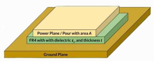
In modern PCB design, effective signal integrity demands careful attention to power distribution and return paths. PCB copper pour grounding emerges as a fundamental technique, where unused copper areas on signal layers connect to a ground net, forming a distributed ground plane. This approach lowers impedance, stabilizes voltage references, and mitigates electromagnetic interference. Copper pour noise reduction further enhances performance by providing shielding and reducing crosstalk between adjacent traces. For electric engineers working on high-speed circuits, mastering these methods ensures compliance with reliability standards and optimizes overall board functionality. Ground plane copper pour, in particular, transforms fragmented layouts into cohesive low-inductance structures essential for multi-layer boards.
Copper pours also aid thermal dissipation by increasing copper mass, which spreads heat evenly across the board. However, improper implementation can introduce parasitic effects or manufacturing challenges. Engineers must balance connectivity, clearances, and layer stackup to achieve optimal results. This article explores structured techniques for PCB copper pour grounding, copper pour noise reduction, and minimizing ground loops copper pour, drawing on established design principles.
What Is PCB Copper Pour and Why It Matters
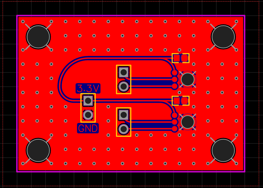
PCB copper pour refers to the process of filling open areas on copper layers with solid copper regions during layout. These regions typically connect to a designated net, most commonly ground, creating an extensive conductive plane. In two-layer boards, this compensates for the absence of dedicated inner planes, while in multi-layer designs, it reinforces existing ground layers. The primary goal of PCB copper pour grounding lies in providing a low-impedance return path for currents, which minimizes voltage drops and inductive noise.
Beyond grounding, copper pour contributes to mechanical stability by reducing warpage during fabrication and assembly. It also supports shielding, where the plane acts as a Faraday cage for sensitive signals routed above or below. For noise-sensitive applications like RF or mixed-signal circuits, copper pour noise reduction becomes critical, as fragmented ground paths amplify crosstalk and radiated emissions. Industry guidelines emphasize uniform pours to maintain consistent electrical properties across the board.
Electric engineers appreciate how ground plane copper pour integrates seamlessly with impedance-controlled traces. Without it, return currents spread out, increasing loop areas and susceptibility to external fields. Proper pours ensure predictable behavior, aligning with performance specifications in high-density interconnects.
Technical Principles Behind Copper Pour Grounding
Ground currents in PCBs seek the path of least impedance, spreading across available copper under the signal traces. A solid copper pour connected to ground facilitates this by offering a broad, low-inductance surface parallel to the signals. This configuration reduces partial inductance compared to thin traces alone, as the plane distributes current evenly. According to IPC-2221B, design principles for printed boards stress the importance of continuous conductive planes for stable reference potentials.
The capacitive coupling between signal traces and the underlying pour further stabilizes voltages, filtering high-frequency noise. At gigahertz frequencies, skin effect confines currents to the plane's surface, enhancing effectiveness. However, gaps or islands in the pour disrupt current flow, creating high-impedance spots that foster noise. Engineers model these effects using field solvers to verify pour integrity before fabrication.
Thermal expansion differences between copper and substrate materials influence pour reliability. Uniform pours minimize stress concentrations, preventing delamination over temperature cycles. This principle extends to minimizing ground loops copper pour, where multiple ground connections form unintended current paths, inducing voltages via magnetic coupling.
Mechanisms of Noise Reduction with Copper Pour
Noise in PCBs arises from switching transients, crosstalk, and external coupling, all exacerbated by poor return paths. Copper pour noise reduction leverages the plane's low impedance to shunt these disturbances to ground swiftly. The plane's distributed capacitance absorbs high-frequency components, while its resistance damps resonances. In mixed-signal designs, separating analog and digital pours prevents noise migration, though careful stitching maintains overall integrity.
Electromagnetic shielding occurs as the pour reflects or absorbs fields from nearby traces. For microstrip lines, the ground plane below defines characteristic impedance and confines fields, reducing radiation. Engineers observe that pours thicker than standard 1 oz/ft2 offer marginal gains but increase etching complexity. Compliance with IPC-6012E ensures the fabricated plane meets performance criteria for continuity and thickness uniformity.
Ground loops form when currents return via disparate paths, picking up interference. Minimizing ground loops copper pour involves solid, unbroken planes that force currents to flow directly under signals, collapsing loop areas to near zero. This technique proves vital in power electronics, where high di/dt generates significant magnetic flux.
Practical Techniques for Effective PCB Copper Pour Grounding
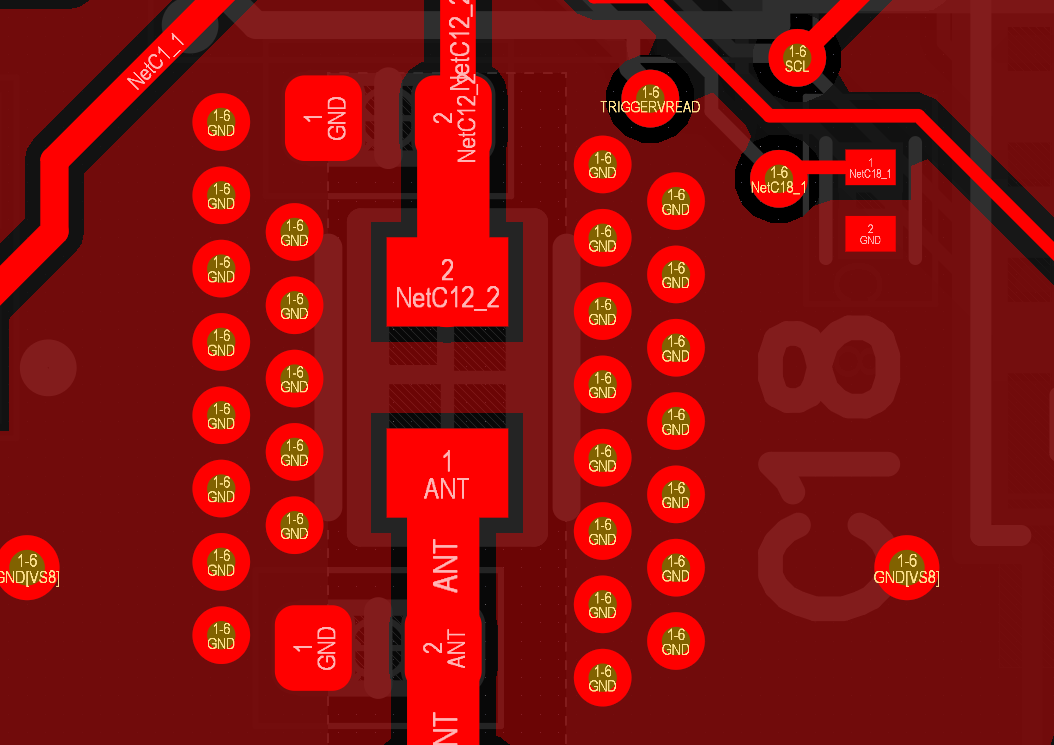
Start with net assignment during layout: designate pours explicitly to the ground net, avoiding accidental connections to power or signals. Use design rules to enforce minimum clearances around traces, typically 10-15 mils depending on voltage and density. Connect isolated pour regions with stitching vias placed every 1/20th wavelength of the highest frequency or closer for power integrity. This via fencing ensures equipotential across the plane, critical for PCB copper pour grounding.
In multi-layer boards, prioritize inner layers for solid ground planes, supplementing outer layers with pours where space allows. Hatch patterns in high-power areas prevent blistering during soldering, while full solids suit signal-heavy zones. Simulate current density to identify hotspots, adjusting via placement accordingly. Ground plane copper pour excels here, as inner pours remain uninterrupted by surface components.
Consider board outline and cutouts: extend pours to edges but relieve around mounting holes to avoid shorts. For flexible-rigid designs, pours must align across flex zones without cracking risks.
Strategies for Copper Pour Noise Reduction
Position bypass capacitors strategically over the pour, leveraging its low inductance for decoupling. Place vias immediately adjacent to IC ground pins, tying them to the pour for shortest paths. Avoid routing signals over pour splits, as these create slot antennas radiating noise. In high-speed designs, tent unused vias in the pour to minimize stubs that reflect signals.
For crosstalk mitigation, maintain pour under differential pairs, ensuring balanced coupling to ground. Copper pour noise reduction shines in reducing simultaneous switching noise, where multiple ICs draw current; the plane equalizes potentials across the board. Monitor impedance profiles post-layout to confirm pour contributions.
Layer sequencing impacts efficacy: ground-signal-ground stackups sandwich signals between planes, maximizing shielding. Alternate pours on adjacent layers if full planes unavailable.
Best Practices for Ground Plane Copper Pour and Minimizing Ground Loops
Adopt a single ground net policy unless isolation required, preventing digital-analog loop interactions. Use spokes or spokes-with-rims for power pours coupling to ground, minimizing stray capacitances. In chassis-grounded systems, isolate board ground via capacitors to break DC loops while passing RF. Minimizing ground loops copper pour demands via stitching around sensitive areas, forcing local returns.
Fabrication-aware pours account for etching undercuts: wider features yield better tolerances. Post-etch inspection verifies connectivity per IPC standards. For high-reliability boards, anneal copper to reduce grain boundaries enhancing conductivity.
Common Pitfalls and Troubleshooting
Unconnected pours accumulate charge, acting as antennas worse than voids. Always verify net assignment and run DRCs for orphans. Excessive pours on outer layers trap solder during reflow, causing bridging; use selective hatching. Measure plane impedance post-assembly with TDR to diagnose issues.
Ground bounce signals poor decoupling or pour discontinuities. Scope waveforms at multiple points; add vias if drops exceed thresholds. For EMI failures, review pour uniformity under antennas.
Conclusion
Mastering PCB copper pour grounding transforms layouts from noisy prototypes to robust products. Techniques like stitching, uniform planes, and strategic clearances deliver copper pour noise reduction and effective ground plane copper pour. By minimizing ground loops copper pour, engineers achieve superior signal integrity and EMC compliance. Integrate these practices early in design for optimal results, ensuring boards perform reliably in demanding environments.
FAQs
Q1: What is PCB copper pour grounding and its benefits?
A1: PCB copper pour grounding involves connecting filled copper areas to the ground net, creating a low-impedance plane. Benefits include reduced return path inductance, stable voltage references, and lower EMI susceptibility. This technique supports high-speed signals by minimizing voltage noise and improving thermal distribution. Electric engineers use it routinely for reliable multi-layer designs.
Q2: How does copper pour noise reduction work in practice?
A2: Copper pour noise reduction functions by providing capacitive shunting and shielding for traces. The plane absorbs transients and confines fields, cutting crosstalk in dense layouts. Place decoupling capacitors over pours and stitch with vias for best results. Avoid splits to prevent resonances.
Q3: Why is ground plane copper pour essential for high-frequency circuits?
A3: Ground plane copper pour offers a broad reference for impedance control and return currents at high frequencies. It collapses loop areas, reducing radiation and susceptibility. Stitching ensures continuity, aligning with design standards. This setup is critical for RF and digital interfaces.
Q4: What techniques help in minimizing ground loops with copper pour?
A4: Minimizing ground loops with copper pour requires solid, single-point referenced planes with dense via stitching. Avoid multiple ground returns; use single net connections. Simulate loop areas and add guards around analog sections. This prevents induced voltages in mixed-signal boards.
References
IPC-2221B - Generic Standard on Printed Board Design. IPC, 2009
IPC-6012E - Qualification and Performance Specification for Rigid Printed Boards. IPC, 2017


